Table 2b. i, C switch routing control registers for the max9135 – Rainbow Electronics MAX9135 User Manual
Page 11
MAX9132/MAX9134/MAX9135
I
2
C Interface
The MAX9132/MAX9134/MAX9135 operate as slaves
that send and receive data through I
2
C (see Figure 1).
The interface uses a serial-data line (SDA) and a serial-
clock line (SCL) to achieve bidirectional communication
between master(s) and slave(s). A master (typically a
microcontroller) initiates all data transfers to and from
the slave and generates the SCL clock that synchro-
nizes the data transfer. The SDA line operates as both
an input and an open-drain output. A pullup resistor,
typically 4.7k
Ω, is required on SDA. The SCL line oper-
ates only as an input. A pullup resistor is required on
SCL if there are multiple masters on the I
2
C interface, or
if the master in a single-master system has an open-
drain SCL output. Each transmission consists of a
START condition sent by a master, followed by the 7-bit
slave address plus R/W bit, a register address byte, a
data byte, and finally a STOP condition. Table 3 shows
the slave address selection by the AS0 and AS1 pins.
Data Format for Writing to the Slave
A write to the MAX9132/MAX9134/MAX9135 comprises
the transmission of the slave address with the R/
W bit
set to 0, followed by at least 1 byte of information. The
first byte of information is the command byte. The com-
mand byte determines which registers of the
MAX9132/MAX9134/MAX9135 are to be written by the
next byte, if received. If a STOP condition is detected
after the command byte is received, the MAX9132/
MAX9134/MAX9135 take no further action beyond stor-
ing the command byte. Any bytes that are received
after the command byte are data bytes. The first data
byte goes into the internal register of the crossbar
switch selected by the command byte (Figure 2). If
Programmable, High-Speed, Multiple
Input/Output LVDS Crossbar Switches
______________________________________________________________________________________
11
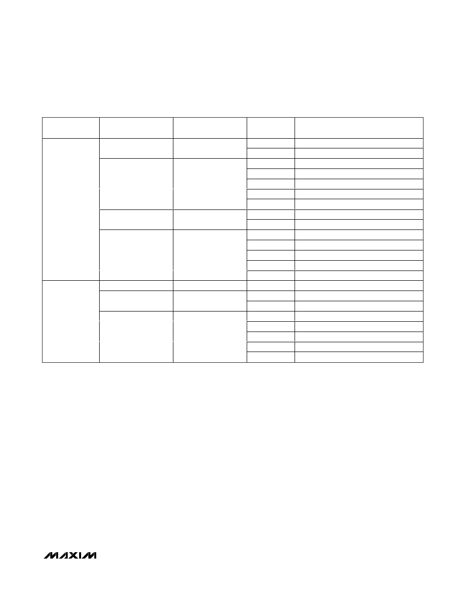
REGISTER
ADDRESS
REGISTER BIT(S)
DESCRIPTION
VALUE
FUNCTION
0
DOUT1 preemphasis off
D7
DOUT1 Preemphasis
1
DOUT1 preemphasis on
000
DOUT1 not connected
001
DOUT1 connected to DIN1
010
DOUT1 connected to DIN0
011
DOUT1 connected to DIN2
D[6:4]
DOUT1 Routing
Connection
100
DOUT1 connected to DIN3
0
DOUT0 preemphasis off
D3
DOUT0 Preemphasis
1
DOUT0 preemphasis on
000
DOUT0 not connected
001
DOUT0 connected to DIN1
010
DOUT0 connected to DIN0
011
DOUT0 connected to DIN2
0x01
D[2:0]
DOUT0 Routing
Connection
100
DOUT0 connected to DIN3
D[7:4]
Reserved
0000
Set these bits to 0000
0
DOUT2 preemphasis off
D3
DOUT2 Preemphasis
1
DOUT2 preemphasis on
000
DOUT2 not connected
001
DOUT2 connected to DIN1
010
DOUT2 connected to DIN0
011
DOUT2 connected to DIN2
0x02
D[2:0]
DOUT2 Routing
Connection
100
DOUT2 connected to DIN3
Table 2b. I
2
C Switch Routing Control Registers for the MAX9135