Rainbow Electronics MAX9135 User Manual
Page 2
MAX9132/MAX9134/MAX9135
Programmable, High-Speed, Multiple
Input/Output LVDS Crossbar Switches
2
_______________________________________________________________________________________
ABSOLUTE MAXIMUM RATINGS
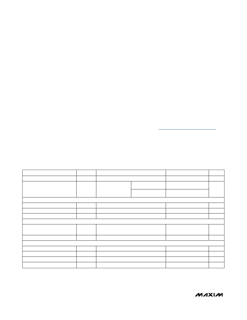
DC ELECTRICAL CHARACTERISTICS
(V
AVDD
= V
DVDD
= V
LVDSVDD
= +3.0V to +3.6V, T
A
= -40°C to +105°C, unless otherwise noted. Typical values are at V
AVDD
= V
DVDD
= V
LVDSVDD
= +3.3V, T
A
= +25°C.) (Note 2)
Stresses beyond those listed under “Absolute Maximum Ratings” may cause permanent damage to the device. These are stress ratings only, and functional
operation of the device at these or any other conditions beyond those indicated in the operational sections of the specifications is not implied. Exposure to
absolute maximum rating conditions for extended periods may affect device reliability.
V
DD
to GND ...........................................................-0.3V to +4.0V
All Pins to GND .............................................-0.3V to V
DD
+ 0.3V
Short-Circuit Duration (all outputs).............................Continuous
Continuous Power Dissipation (T
A
= +70°C)
32-Pin TQFP (derate 27.8mW/°C above +70°C)........2222mW
20-Pin TSSOP (derate 26.5mW/°C above +70°C) .....2122mW
Junction-to-Case Thermal Resistance (
θ
JC
) (Note 1)
32-Pin TQFP ...................................................................4°C/W
20-Pin TSSOP.................................................................2°C/W
Junction-to-Ambient Thermal Resistance (
θ
JA
) (Note 1)
32-Pin TQFP .................................................................36°C/W
20-Pin TSSOP............................................................37.7°C/W
Operating Temperature Range .........................-40°C to +105°C
Junction Temperature ......................................................+150°C
Storage Temperature Range .............................-65°C to +150°C
ESD Protection
Human Body Model (RD = 1.5kΩ, CS = 100pF)
All Other Pins Including SCL, SDA to GND .................±2kV
IEC61000-4-2 (RD = 330Ω, CS = 150pF)
Contact Discharge
(DIN_, DOUT_) to GND ..............................................±10kV
Ai-Gap Discharge
(DIN_, DOUT_) to GND ..............................................±15kV
ISO10605 (RD = 2kΩ, CS = 330pF)
Contact Discharge
(DIN_, DOUT_) to GND ..............................................±10kV
Ai-Gap Discharge
(DIN_, DOUT_) to GND ..............................................±25kV
Lead Temperature (soldering, 10s) ................................+300°C
PARAMETER
SYMBOL
CONDITIONS
MIN
TYP
MAX
UNITS
Supply Voltage
V
DD
3.0
3.6
V
MAX9132
60
80
Supply Current
I
AVDD
,
I
DVDD
,
I
LVDSVDD
Outputs switching at
20MHz
MAX9134/MAX9135
86
100
mA
SINGLE-ENDED CMOS INPUTS (
PD, FS, RXD)
Input High Level
V
IH1
2.0
V
Input Low Level
V
IL1
0.8
V
Input High Current
I
IN1
V
IN
= 0 to V
DD
-20
+20
µA
SINGLE-ENDED OUTPUTS (TXD, AS1/NSLP)
Output High Level
V
OH
V
DD
-
0.4
V
Output Low Level
V
OL
I
OL
= 4mA
0.4
V
3-LEVEL INPUTS (S5–S0, AS0, AS1)
Input High Level
V
IH3
2.5
V
Input Low Level
V
IL3
0.8
V
Input Open Level
V
IO3
Measured at the input pins
1.2
1.45
1.9
V
Input Current
I
L3
, I
H3
V
IL3
= 0 or V
IH3
= V
DD
-20
+20
µA
Note 1: Package thermal resistances were obtained using the method described in JEDEC specification JESD51-7, using a four-
layer board. For detailed information on package thermal considerations, refer to
www.maxim-ic.com/thermal-tutorial
.