Applications information, Table 5. register 0x00 error flag mapping for lin – Rainbow Electronics MAX9135 User Manual
Page 13
MAX9132/MAX9134/MAX9135
Programmable, High-Speed, Multiple
Input/Output LVDS Crossbar Switches
______________________________________________________________________________________
13
MAX9135 LSB first, up to a maximum data rate of
20kbps. The LIN slave node waits for the synchronization
pulse, then synchronizes itself to the pulse. The node
must then read the identifier and send/receive data bytes
to the master, setting the error flag register when neces-
sary. The LIN interface uses the same routing function of
the switch control registers (0x01, 0x02) as the I
2
C inter-
face. The routing action takes place after correct check-
sum verification. The LIN status register (0x00) holds the
error flags for the LIN transceiver. For a write, the master
writes 2 bytes of data to the registers (0x01, 0x02). For a
read, the slave outputs the contents of registers 0x00,
0x01, and 0x02, along with the stuffing byte at a constant
value (0xFF). In either mode, the checksum follows at the
end of the data bytes. Figure 3 shows the write and read
signal frame format. Figure 4 shows the LIN write and
read data frame.
LIN-Protected Identifier
The LIN bus uses the 8-bit protected identifier (PID) to
address the slave nodes. Two parity bits (MSBs) along
with 6 ID bits (LSBs) make up the PID field. Table 4
defines the sets of the identifiers for the write/read
operations of the LIN slave node. AS0 selects the iden-
tifiers. AS1/NSLP becomes the NSLP output for activat-
ing the LIN driver chip (MAX13020).
LIN Error Handling
Register 0x00 contains the error flags found in the LIN
signal by the slave note (Table 5). A successful LIN
read resets register 0x00.
Pin Control by S[5:0] (MAX9134/MAX9135)
The programming pins S[5:0] initially set the switch
routing upon power-up, while the device latches the
state of these pins. The I
2
C interface can override the
power-on state later. Table 6a gives the details of the
routing control for the MAX9134. Table 6b gives the
details of the routing control for the MAX9135.
Applications Information
3-Level Inputs
The MAX9132/MAX9134/MAX9135 use several 3-level
inputs to control the device. Use three-state logic to
realize the 3-level logic using digital control.
Alternatively, if a high-impedance output is unavailable,
apply a voltage of V
DD
/2 to realize the midlevel high-
impedance state.
WRITE ID
READ ID
AS0
ID[5:0]
PID FIELD
ID[5:0]
PID FIELD
Low
0x08
0x08
0x27
0xE7
Open
0x0A
0xCA
0x29
0xE9
High
0x1C
0x9C
0x2B
0x2B
Table 4. LIN Identifiers for Write and Read Operations
REGISTER BIT(S)
DESCRIPTION
FUNCTION
D[7:5]
Reserved
Reserved
D4
Sync
Sync pulse widths outside the given tolerances detected
D3
Transmit
Value read on RXD different from value transmitted on TXD during a read
D2
Checksum
Checksum sent during a write does not match the expected checksum
D1
Parity
ID parity bit does not match expected parity
D0
Frame
Message frame did not complete within the maximum allowed time
Table 5. Register 0x00 Error Flag Mapping for LIN
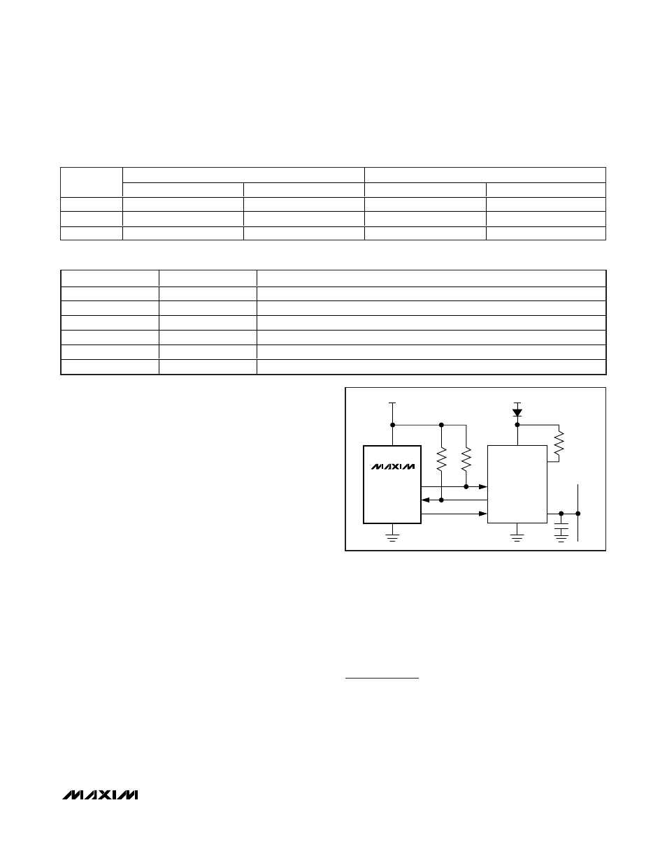
MAX9132
MAX9134
MAX9135
V
BAT
MAX13020
V
DD
INH
TXD
RXD
NSLP
LIN
BUS
TXD
5k
Ω
5k
Ω
5k
Ω
RXD
NSLP
NWAKE
LIN
Figure 5. Connecting the MAX9132/MAX9134/MAX9135 to the
MAX13020