Table 2a. i – Rainbow Electronics MAX9135 User Manual
Page 10
MAX9132/MAX9134/MAX9135
Programmable, High-Speed, Multiple
Input/Output LVDS Crossbar Switches
10
______________________________________________________________________________________
REGISTER
ADDRESS
REGISTER BIT(S)
DESCRIPTION
VALUE
FUNCTION
0
DOUT1 preemphasis off
D7
DOUT1 Preemphasis
1
DOUT1 preemphasis on
000
DOUT1 in high impedance
001
DOUT1 connected to DIN1
010
DOUT1 connected to DIN0
D[6:4]
DOUT1 Routing
Connection
011
DOUT1 connected to DIN2
0
DOUT0 preemphasis off
D3
DOUT0 Preemphasis
1
DOUT0 preemphasis on
000
DOUT0 in high impedance
001
DOUT0 connected to DIN1
010
DOUT0 connected to DIN0
0x01
D[2:0]
DOUT0 Routing
Connection
011
DOUT0 connected to DIN2
0
DOUT3 preemphasis off
D7
DOUT3 Preemphasis
1
DOUT3 preemphasis on
000
DOUT3 in high impedance
001
DOUT3 connected to DIN1
010
DOUT3 connected to DIN0
D[6:4]
DOUT3 Routing
Connection
011
DOUT3 connected to DIN2
0
DOUT2 preemphasis off
D3
DOUT2 Preemphasis
1
DOUT2 preemphasis on
000
DOUT2 in high impedance
001
DOUT2 connected to DIN1
010
DOUT2 connected to DIN0
0x02
(MAX9134 only)
D[2:0]
DOUT2 Routing
Connection
011
DOUT2 connected to DIN2
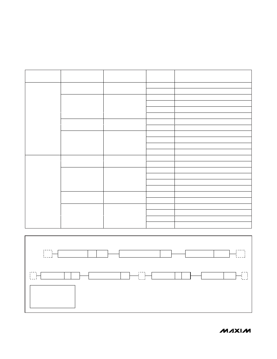
Table 2a. I
2
C/LIN Switch Routing Control Registers for the MAX9132/MAX9134
BIT 7…………….……………… BIT 0 ACK BIT BIT 7…………….…………………BIT 0 ACK BIT
8-BIT DATA
AS
BIT 7…….…….…………BIT 0 ACK BIT
7-BIT SLAVE ID
0
AS
ADDR
AS
ADDRESS/COMMAND BYTE
S
P
SINGLE WRITE
SINGLE READ
BIT 7…………….……….BIT 0 ACK BIT
BIT 7………….…………BIT 0 ACK BIT
BIT 7…………….……………BIT 0 ACK BIT
8-BIT DATA
/AM
BIT 7…….…………BIT 0 ACK BIT
7-BIT SLAVE ID
0
AS
ADDR
AS
S
7-BIT SLAVE ID
1
AS
ADDRESS/COMMAND BYTE
S
P
ADDR: 8-BIT REGISTER ADDRESS
S: 2-WIRE BUS START CONDITION BY MASTER
P: 2-WIRE BUS STOP CONDITION BY MASTER
AS: ACKNOWLEDGE BY SLAVE
AM: ACKNOWLEDGE BY MASTER
/AM: NO ACKNOWLEDGE BY MASTER
Figure 2. Single-Byte Write and Single-Byte Read