Rainbow Electronics MAX9135 User Manual
Page 16
MAX9132/MAX9134/MAX9135
Input/Output Termination
Terminate LVDS inputs/outputs through 100
Ω differen-
tial termination, or use an equivalent Thevenin termina-
tion. Terminate both inputs/outputs and use identical
terminations on each for the lowest output-to-output
skew.
Power-Supply Bypassing
Adequate power-supply bypassing is necessary to
maximize the performance and noise immunity. Bypass
each supply to their respective grounds with high-
frequency surface-mount 0.01µF ceramic capacitors as
close as possible to the device. Use multiple bypass
vias for connection to minimize inductance.
Board Layout
Separate the I
2
C/LIN signals and LVDS signals to pre-
vent crosstalk. When possible, use a four-layer PCB
with separate layers for power, ground, LVDS, and digi-
tal signals. Layout PCB traces for 100
Ω differential
characteristic impedance. The trace dimensions
depend on the type of trace used (microstrip or
stripline).
Route the PCB traces for an LVDS channel (there are
two conductors per LVDS channel) in parallel to main-
tain the differential characteristic impedance. Place the
100
Ω (typ) termination resistor at both ends of the
LVDS driver and receiver. Avoid vias. If vias must be
used, use only one pair per LVDS channel and place
the via for each line at the same point along the length
of the PCB traces. This way, any reflections occur at
the same time. Do not make vias into test points for
automated test equipment. Make the PCB traces that
make up a differential pair the same length to avoid
skew within the differential pair.
Cables and Connectors
Interconnect for LVDS typically has a differential
impedance of 100
Ω. Use cables and connectors that
have matched differential impedance to minimize
impedance discontinuities. Twisted-pair and shielded
twisted-pair cables offer superior signal quality com-
pared to ribbon cable and tend to generate less EMI
due to magnetic-field-canceling effects. Balanced
cables pick up noise as common mode that is rejected
by the LVDS receiver. Add a 0.1µF capacitor in series
with each output for AC-coupling.
Choosing Pullup Resistors
I
2
C requires pullup resistors to provide a logic-high
level to data and clock lines. There are tradeoffs
between power dissipation and speed, and a compro-
mise must be made in choosing pullup resistor values.
Every device connected to the bus introduces some
capacitance even when the device is not in operation.
I
2
C specifies 300ns rise times to go from low to high
(30% to 70%) for fast mode, which is defined for a data
rate up to 400kbps (see the
I
2
C Interface
section for
details). To meet the rise time requirement, choose the
pullup resistors so that the rise time t
R
= 0.85R
PULLUP
x
C
BUS
< 300ns. If the transition time becomes too slow,
the setup and hold times may not be met and wave-
forms are not recognized.
Programmable, High-Speed, Multiple
Input/Output LVDS Crossbar Switches
16
______________________________________________________________________________________
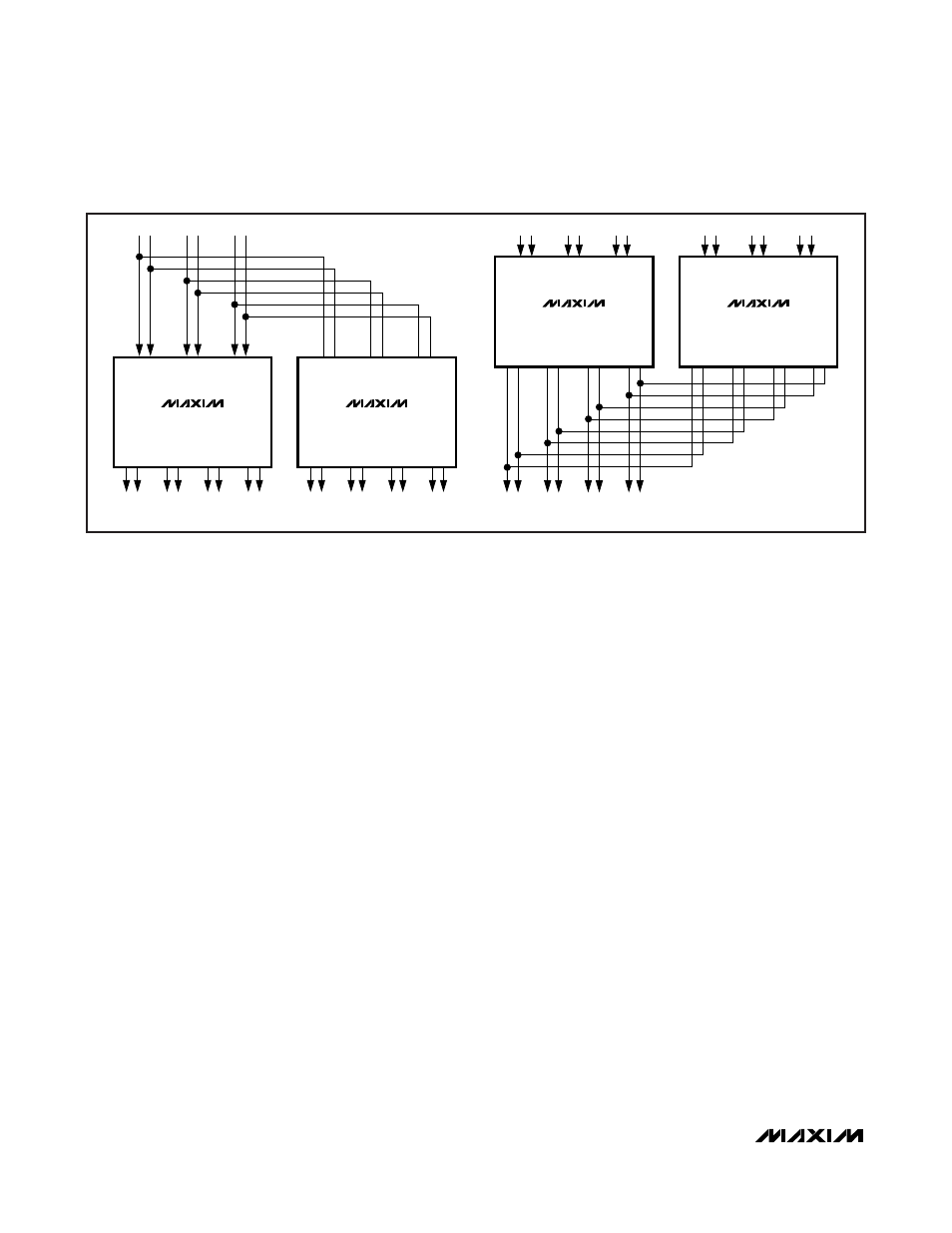
3 x 8 SWITCH
6 x 4 SWITCH
DOUT1
DOUT2
DOUT3
DOUT4
DIN1
DIN2
DIN3
MAX9134
DOUT1
DOUT2
DOUT3
DOUT4
DIN1
DIN2
DIN3
MAX9134
DOUT1
DOUT2
DOUT3
DOUT4
DIN1
DIN2
DIN3
MAX9134
DOUT1
DOUT2
DOUT3
DOUT4
DIN1
DIN2
DIN3
MAX9134
Figure 7. Topologies for Port Expansion