Pin description, Typical operating characteristics (continued) – Rainbow Electronics MAX9135 User Manual
Page 6
Pin Description
PIN
MAX9132
TSSOP
MAX9134
TQFP
MAX9135
TQFP
NAME
FUNCTION
1
31
30
PD
P ow er - D ow n Inp ut.
P D = l ow for p ow er - d ow n. P D = hi g h for p ow er - up w i thout
p r eem p hasi s. Leave
P D op en for p ow er - up w i th p r eem p hasi s on al l outp uts.
2
32
31
DVDD
Digital Power Supply. Bypass DVDD to DGND with 0.1µF and 0.01µF
capacitors as close as possible to the device.
3
1
1
DIN0+
Port 0 Positive Input
4
2
2
DIN0-
Port 0 Negative Input
5
3
3
DIN1+
Port 1 Positive Input
6
4
4
DIN1-
Port 1 Negative Input
—
5
—
AGND
Analog Ground
7
6
5
DIN2+
Port 2 Positive Input
8
7
6
DIN2-
Port 2 Negative Input
—
—
7
DIN3+
Port 3 Positive Input
—
—
8
DIN3-
Port 3 Negative Input
9
8
9
AVDD
Analog Power Supply. Bypass AVDD to AGND with 0.1µF and 0.01µF
capacitors as close as possible to the device.
10
—
—
FS
I
2
C and LIN Interface Selection Input. FS = low for LIN, FS = high for I
2
C.
—
9
10
S0
Routing Selection 0 Input. See Tables 6a and 6b.
—
10
11
S1
Routing Selection 1 Input. See Tables 6a and 6b.
—
11
12
S2
Routing Selection 2 Input. See Tables 6a and 6b.
—
12
13
S3
Routing Selection 3 Input. See Tables 6a and 6b.
11
13
14
AS0
3-Level I
2
C Address Selection 0 Input (Table 3) or LIN Identifier Selection 0
Input (Table 4)
MAX9132/MAX9134/MAX9135
Programmable, High-Speed, Multiple
Input/Output LVDS Crossbar Switches
6
_______________________________________________________________________________________
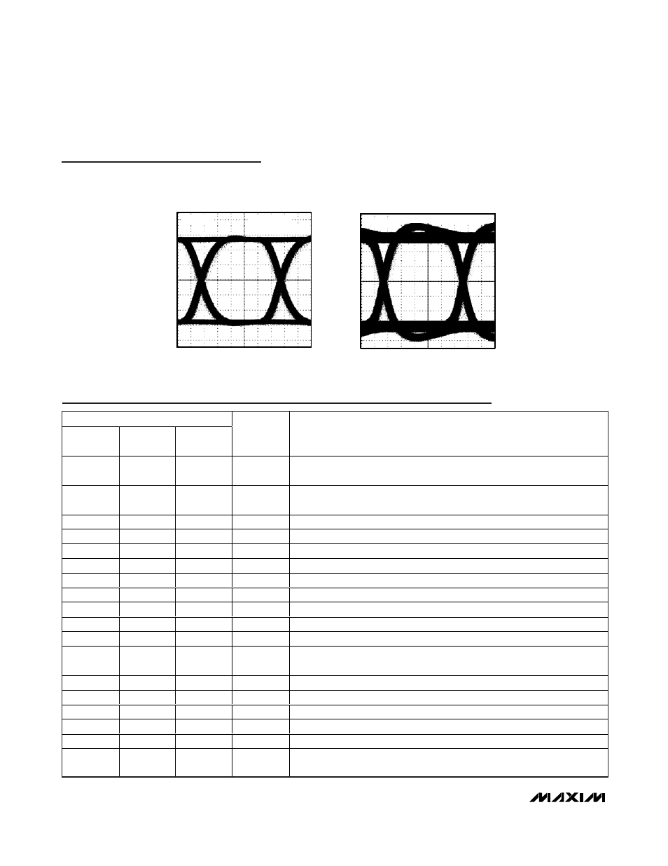
Typical Operating Characteristics (continued)
(V
AVDD
= V
DVDD
= V
LVDSVDD
= +3.3V, T
A
= +25°C, unless otherwise noted.)
OV
200ps/div
EYE DIAGRAM
MAX9132/4/5 toc10
150mV/div
840Mbps PRBS
NO PREEMPHASIS
OV
200ps/div
EYE DIAGRAM
MAX9132/4/5 toc11
150mV/div
840Mbps PRBS WITH PREEMPHASIS