Vishay semiconductors – C&H Technology EMF050J60U User Manual
Page 6
VS-EMF050J60U
www.vishay.com
Vishay Semiconductors
Revision: 09-Dec-11
5
Document Number: 93494
For technical questions within your region:
,
,
THIS DOCUMENT IS SUBJECT TO CHANGE WITHOUT NOTICE. THE PRODUCTS DESCRIBED HEREIN AND THIS DOCUMENT
ARE SUBJECT TO SPECIFIC DISCLAIMERS, SET FORTH AT
www.vishay.com/doc?91000
Note
(1)
Energy losses include “tail” and diode reverse recovery.
Note
(1)
Mounting surface flat, smooth, and greased
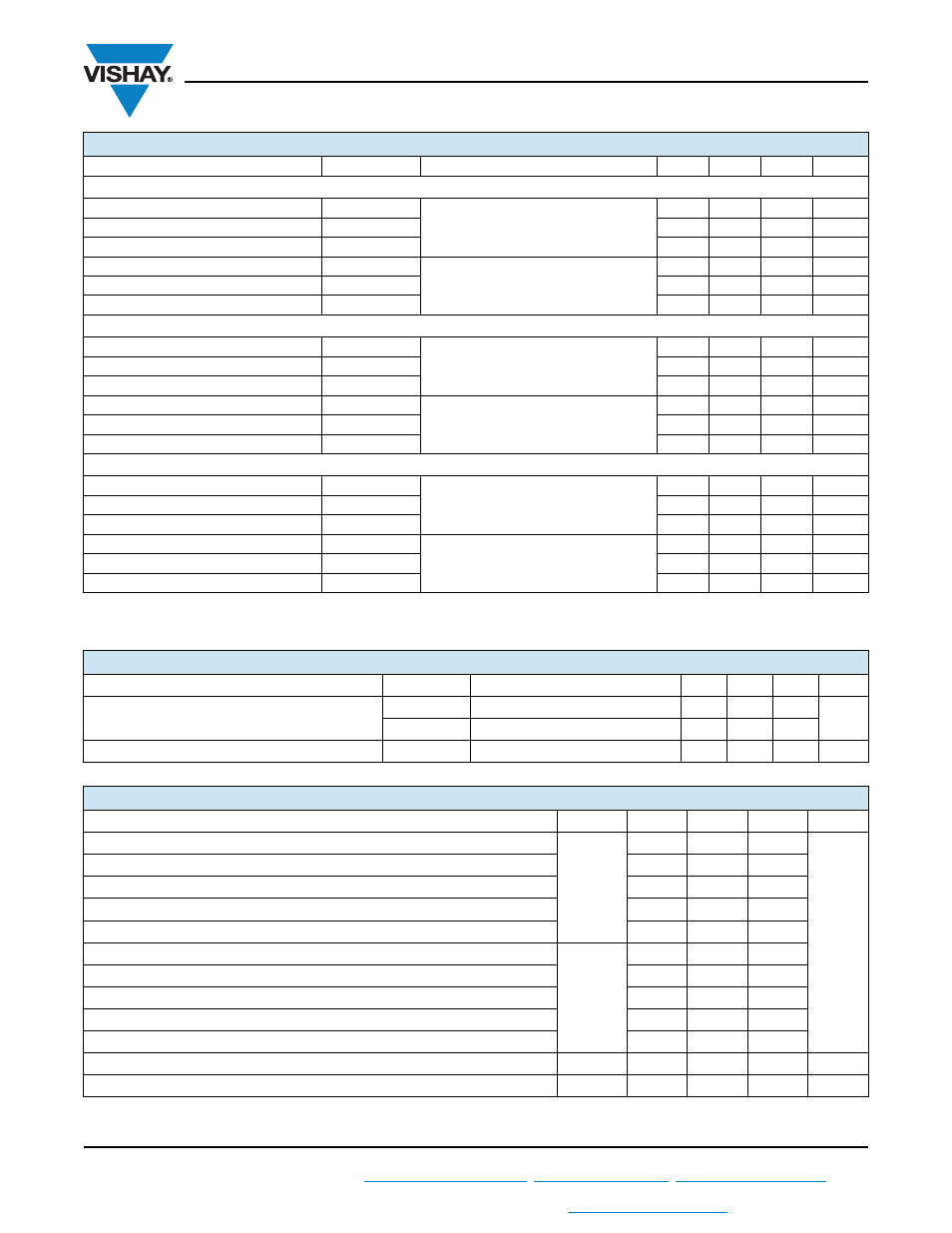
D1 - D2 CLAMPING DIODE
Diode reverse recovery time
t
rr
V
R
= 200 V
I
F
= 30 A
dl/dt = 500 A/μs
-
50
80
ns
Diode peak reverse current
I
rr
-
7.5
11
A
Diode recovery charge
Q
rr
-
185
440
nC
Diode reverse recovery time
t
rr
V
R
= 200 V
I
F
= 30 A
dl/dt = 500 A/μs, T
J
= 125 °C
-
107
147
ns
Diode peak reverse current
I
rr
-
18
22
A
Diode recovery charge
Q
rr
-
955
1620
nC
D3 - D4 AP DIODE
Diode reverse recovery time
t
rr
V
R
= 400 V
I
F
= 50 A
dl/dt = 500 A/μs
-
114
150
ns
Diode peak reverse current
I
rr
-
21
25
A
Diode recovery charge
Q
rr
-
1200
1875
nC
Diode reverse recovery time
t
rr
V
R
= 400 V
I
F
= 50 A
dl/dt = 500 A/μs, T
J
= 125 °C
-
170
210
ns
Diode peak reverse current
I
rr
-
28
32
A
Diode recovery charge
Q
rr
-
2160
3360
nC
D5 - D6 AP DIODE
Diode reverse recovery time
t
rr
V
R
= 200 V
I
F
= 30 A
dl/dt = 500 A/μs
-
46
77
ns
Diode peak reverse current
I
rr
-
7
11
A
Diode recovery charge
Q
rr
-
161
423
nC
Diode reverse recovery time
t
rr
V
R
= 200 V
I
F
= 30 A
dl/dt = 500 A/μs, T
J
= 125 °C
-
106
138
ns
Diode peak reverse current
I
rr
-
17
22
A
Diode recovery charge
Q
rr
-
900
1518
nC
THERMISTOR ELECTRICAL CHARACTERISTICS (T
J
= 25 °C unless otherwise noted)
PARAMETER SYMBOL
TEST
CONDITIONS
MIN.
TYP.
MAX.
UNITS
Resistance
R
25
4500
5000
5500
R
100
T
J
= 100 °C
468
493
518
B value
B
T
J
= 25 °C/T
J
= 50 °C
3206
3375
3544
K
THERMAL AND MECHANICAL SPECIFICATIONS
PARAMETER SYMBOL
MIN.
TYP.
MAX.
UNITS
Q1 - Q4 IGBT - Junction to case thermal resistance (per switch)
R
thJC
-
-
0.37
°C/W
Q2 - Q3 IGBT - Junction to case thermal resistance (per switch)
-
-
0.37
D1 - D2 Clamping diode - Junction to case thermal resistance (per diode)
-
-
0.83
D3 - D4 AP diode - Junction to case thermal resistance (per diode)
-
-
0.71
D5 - D6 AP diode - Junction to case thermal resistance (per diode)
-
-
1.3
Q1 - Q4 IGBT - Case to sink thermal resistance (per switch)
R
thCS
(1)
-
0.31
-
Q2 - Q3 IGBT - Case to sink thermal resistance (per switch)
-
0.31
-
D1 - D2 Clamping diode - Case to sink thermal resistance (per diode)
-
0.51
-
D3 - D4 AP diode - Case to sink thermal resistance (per diode)
-
0.41
-
D5 - D6 AP diode - Case to sink thermal resistance (per diode)
-
0.62
-
Mounting torque (M4)
-
2
3
Nm
Weight
-
39
-
g
SWITCHING CHARACTERISTICS (T
J
= 25 °C unless otherwise noted)
PARAMETER
SYMBOL
TEST CONDITIONS
MIN.
TYP.
MAX.
UNITS