Adv ance informa t ion, Tms320 second generation devices, Timing diagrams – Texas Instruments TMS320 User Manual
Page 41: Clock timing

TMS320 SECOND GENERATION
DEVICES
SPRS010B — MAY 1987 — REVISED NOVEMBER 1990
POST OFFICE BOX 1443
HOUSTON, TEXAS 77001
41
TIMING DIAGRAMS
This section contains all the timing diagrams for the TMS320 second-generation devices. Refer to the top corner
of page for the specific device.
Timing measurements are referenced to and from a low voltage of 0.8 voltage and a high voltage of 2 volts,
unless otherwise noted.
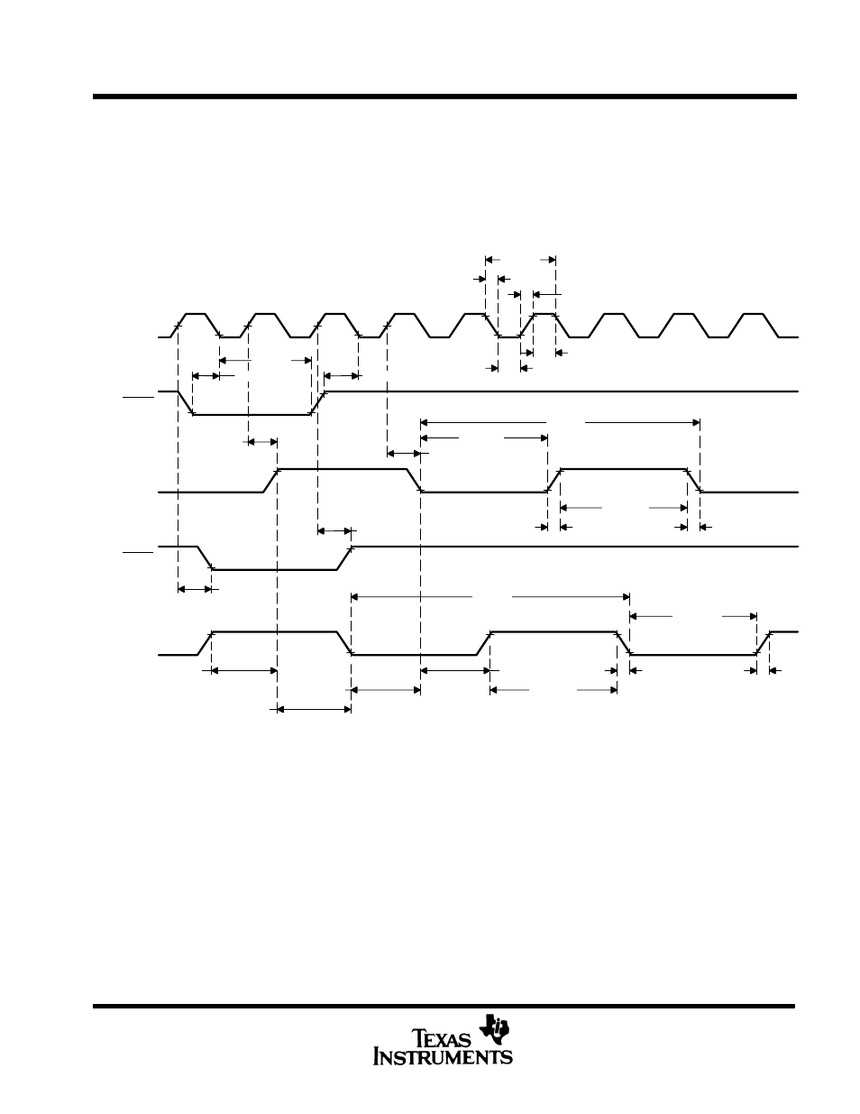
clock timing
X/2CLKIN
SYNC
CLKOUT1
STRB
CLKOUT2
t
c(CI)
t
f(CI)
t
r(CI)
t
w(CIH)
t
w(CIL)
t
h(S)
t
su(S)
t
d(CIH-C)
t
d(CIH-C)
t
w(CL)
t
c(C)
t
w(CH)
t
f(C)
t
r(C)
t
d(CIH-C)
t
c(C)
t
w(CL)
t
r(C)
t
f(C)
t
w(CH)
t
d(C1-C2)
t
d(CIH-C)
t
d(C1-C2)
t
d(C1-C2)
t
d(C1-C2)
t
su(S)
ADV
ANCE
INFORMA
T
ION
