Adv ance informa t ion, Tms320 second generation digital signal processors – Texas Instruments TMS320 User Manual
Page 23

TMS320 SECOND GENERATION
DIGITAL SIGNAL PROCESSORS
SPRS010B — MAY 1987 — REVISED NOVEMBER 1990
POST OFFICE BOX 1443
HOUSTON, TEXAS 77001
23
timing requirements over recommended operating conditions (see Note 3)
MIN
NOM
MAX
UNIT
t
c(C)
CLKIN cycle time
195
597
ns
t
f(CI)
CLKIN fall time
10
†
ns
t
r(CI)
CLKIN rise time
10
†
ns
t
w(CIL)
CLKIN low pulse duration, t
c(CI)
= 50 ns (see Note 4)
40
ns
t
w(CIH)
CLKIN high pulse duration, t
c(CI)
= 50 ns (see Note 4)
40
ns
t
su(S)
SYNC setup time before CLKIN low
10
Q -- 10
ns
t
h(S)
SYNC hold time from CLKIN low
15
ns
†
Value derived from characterization data and not tested.
NOTES: 3. Q = 1/4t
c(C)
.
4. CLKIN duty cycle [t
r(CI)
+ t
w(CIH)]
/ t
c(CI)
must be within 40-60%.
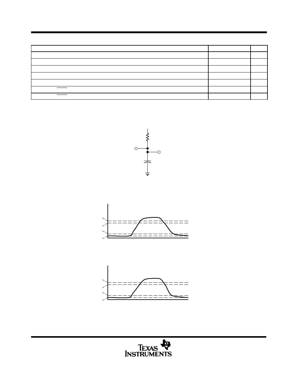
C
L
= 100 pF
2.15 V
R
L
= 825
Test
Point
From Output
Under Test
Figure 3. Test Load Circuit
0.80 V
0.92 V
1.88 V
2.0 V
0
V
IH
(Min)
V
IL
(Max)
(a) Input
0.6 V
0.8 V
2.2 V
2.4 V
0
V
OH
(Min)
V
OL
(Max)
(b) Output
Figure 4. Voltage Reference Levels
ADV
ANCE
INFORMA
T
ION
