Adv ance informa t ion, Tms320 second generation digital signal processors – Texas Instruments TMS320 User Manual
Page 32

TMS320 SECOND GENERATION
DIGITAL SIGNAL PROCESSORS
SPRS010B — MAY 1987 — REVISED NOVEMBER 1990
POST OFFICE BOX 1443
HOUSTON, TEXAS 77001
32
SERIAL PORT TIMING
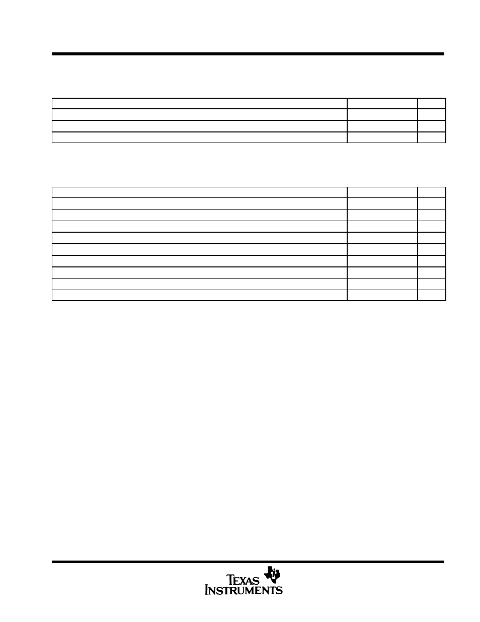
switching characteristics over recommended operating conditions (see Note 3)
PARAMETER
MIN
TYP
MAX
UNIT
t
d(CH-DX)
DX valid after CLKX rising edge (see Note 10)
75
ns
t
d(FL-DX)
DX valid after FSX falling edge (TXM = 0, see Note 10)
40
ns
t
d(CH-FS)
FSX valid after CLKX rising edge (TXM = 1)
40
ns
NOTES: 3. Q = 1/4t
c(C)
.
10. The last occurrence of FSX falling and CLKX rising.
timing requirements over recommended operating conditions (see Note 3)
MIN
NOM
MAX
UNIT
t
c(SCK)
Serial port clock (CLKX/CLKR) cycle time
†
200
ns
t
f(SCK)
Serial port clock (CLKX/CLKR) fall time
25
‡
ns
t
r(SCK)
Serial port clock (CLKX/CLKR) rise time
25
‡
ns
t
w(SCK)
Serial port clock (CLKX/CLKR) low pulse duration (see Note 11)
80
ns
t
w(SCK)
Serial port clock (CLKX/CLKR) high pulse duration (see Note 11)
80
ns
t
su(FS)
FSX/FSR setup time before CLKX/CLKR falling edge (TXM = 0)
18
ns
t
h(FS)
FSX/FSR hold time after CLKX/CLKR falling edge (TXM = 0)
20
ns
t
su(DR)
DR setup time before CLKR falling edge
10
ns
t
h(DR)
DR hold time after CLKR falling edge
20
ns
†
The serial port was tested at a minimum frequency of 1.25 MHz. However, the serial port was fully static but will properly function down
to f
sx
= 0 Hz.
‡
Value derived from characterization data and not tested.
NOTES: 3. Q = 1/4t
c(C)
.
11. The duty cycle of the serial port clock must be within 40-60%.
ADV
ANCE
INFORMA
T
ION
