7 extension connector (j14) – Renesas SH7149 User Manual
Page 42
Operational Specifications
3.1.7 Extension Connector (J14)
Rev.1.0 Dec 15, 2006
3-14
REJ10J0917-0100
3
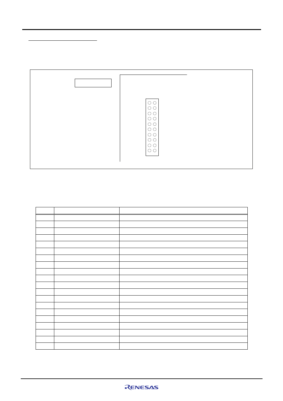
3.1.7 Extension Connector (J14)
Extension connector(J14) connects the pins necessary for writing a on-chip flash memory of SH7149.
Figure 3.1.9 lists pin assignments of the extension connectors.
Board edge
19
20
1
2
J1
4
Top view of the
component side
Board edge
Figure 3.1.9 Pin assignments of the Extension Connector (J14)
Table 3.1.12 lists pin assignments of the extension connector(J14).
Table 3.1.12 Pin assignments of the extension connector (J14)
Pin
Signal name
Other connection
1
RES
________
-
2
GND -
3
FWE
FWE pin Select Jumper (JP2)
4
GND -
5
MD0
DIP switch for system setting (SW4-3)
6
GND -
7
MD1
DIP switch for system setting (SW4-2)
8
GND -
9
NC -
10
GND -
11
NC -
12
GND -
13
NC -
14
GND -
15
FTXD1(PA4/TXD1)*
1
Serial port Select Jumper (JP3), Extension connector(J9, J10)
16
GND -
17
FRXD1(PA3/RXD1)*
2
Serial port Select Jumper (JP4), Extension connector(J9, J10)
18
VCC -
19
NC -
20
VCC -
Note *
1:
When serial port select jumper (JP3) is set to “2-3”, it is activated.
*
2
: When serial port select jumper (JP4) is set to “2-3”, it is activated.