1 functional overview – Renesas SH7149 User Manual
Page 20
Functional Overview
2.1 Functional Overview
Rev.1.0 Dec 15, 2006
2-2
REJ10J0917-0100
2
2.1 Functional Overview
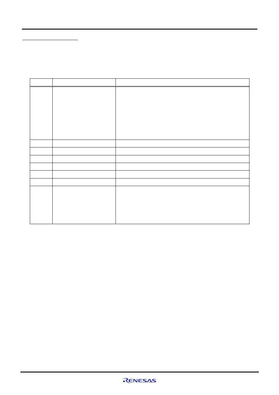
The M3A-HS49 is the SH7149 CPU board that has functions listed in Table2.1.1.
Table2.1.1 lists functional modules of M3A-HS49.
Table2.1.1 Functional Modules of M3A-HS49
Section Function
Content
CPU
SH7149
•
Input(XIN) clock : 10MHz
•
Bus clock : 40MHz, max
•
CPU clock : 80MHz, max
•
On-chip Memory
- Flash memory : 256KB
- RAM : 8KB
2.3
Serial Port Interface
Connects SCI1 of the SH7149 to the Serial Port connector
2.4 Input/Output
Ports
Connects
to the I/O ports of the SH7149
2.5
Clock Module
Controls the system clock
2.6
Reset Module
Controls device reset accommodated by the M3A-HS49
2.7 Interrupt
Switches
Controls interrupt (NMI,IRQ0,MRES)
2.8
E10A-USB Interface
SH7149 H-UDI/AUD interface
- Operational
specifications Connectors, switches and LEDs
•
SH7149 extension connector
•
Switches and LEDs
•
H-UDI connector
Detailed in Chapter 3.