5 user i/o connector (j6-j8), Operational specifications – Renesas SH7149 User Manual
Page 36
Operational Specifications
3.1.5 User I/O Connector (J6-J8)
3
3.1.5 User I/O Connector (J6-J8)
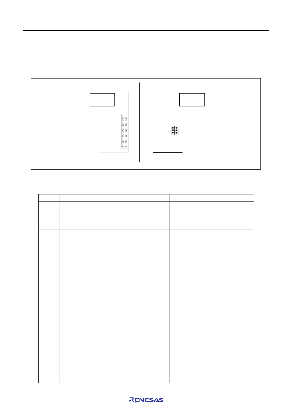
The M3A-HS49 includes user I/O connectors to which the on-chip peripheral function pins of the SH7149 applicable
for motor control (e.g.,MTU2 and AD functions) are connected. Figure3.1.7 shows a pin assignment of each user I/O
connector. Table3.1.6 lists pin assignments of user I/O connector (J6).
1 2
25 26
Board
edge
Board
edge
Top view of the
solder side
J6
Top view of the
component side
Board
edge
Board
edge
J7 J8
1
2
3
1
2
3
Figure3.1.7 Pin Assignment of User I/O Connectors (J6-J8)
Table3.1.6 Pin Assignments of User I/O Connector (J6)
Pin
Signal Name
Other connection
1
+5V
-
2
GND
-
3
PF8/AN8
-
4
PB5/A19/IRQ3/POE5
_________
/TIC5U
Extension Connector(J10)
5
PB3/A17/IRQ1/POE1
_________
/TIC5V Extension
Connector(J10)
6
PB1/BREQ
__________
/TIC5W Extension
Connector(J11)
7
PE9/TIOC3B LED3
8
PE12/TIOC4A LED5
9
PE13/MRES
__________
/TIOC4B MRES
Switch(SW7)
10
PE11/TIOC3D LED4
11
PE14/TIOC4C LED6
12
PE15/IRQOUT
______________
/TIOC4D LED7
13
PE0/TIOC0A LED2
14
PE1/TIOC0B/RXD0 -
15
PE2/TIOC0C/TXD0 -
16
PE3/TIOC0D/SCK0 -
17
PF2/AN2 -
18
PF10/AN10 -
19
PF4/AN4 -
20
PF9/AN9 -
21
PB16/POE3
_________
DIP Switch(SW3)
22
PB17/POE7
_________
DIP Switch(SW3)
23
PF12/AN12 -
24
PF13/AN13 -
25
PF14/AN14 -
26
PF15/AN15 -
Rev.1.0 Dec 15, 2006
3-8
REJ10J0917-0100