7 m3a-hs49 memory mapping – Renesas SH7149 User Manual
Page 14
Overview
1.7 M3A-HS49 Memory Mapping
Rev.1.0 Dec 15, 2006
1-8
REJ10J0917-0100
1
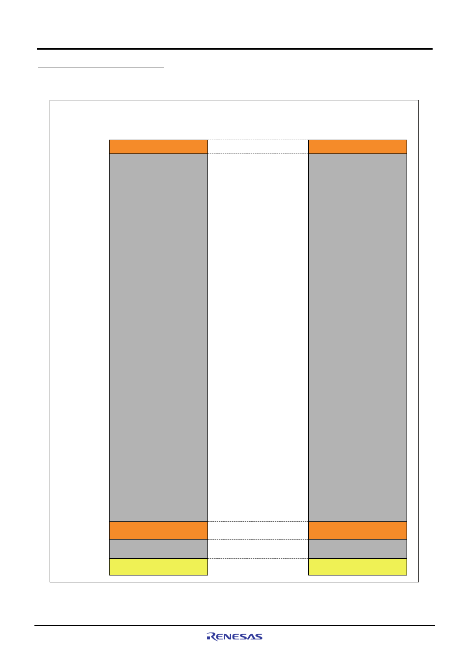
1.7 M3A-HS49 Memory Mapping
Figure1.7.1, Figure1.7.2 and Figure1.7.3 show a memory mapping example of SH7149 in the M3A-HS49.
On-chip ROM(256KB)
Reserved
Logical space of the SH7149
MCU mode 3
(Single Chip mode)
On-chip RAM(8KB)
On-chip Peripheral Module
H’0000 0000
H’FFFF 8FFF
H’FFFF 9000
H’FFFF AFFF
H’FFFF B000
H’FFFF BFFF
H’FFFF C000
H’FFFF FFFF
Memory Mapping
of the M3A-HS49
Reserved
On-chip RAM(8KB)
On-chip Peripheral Module
Reserved
Reserved
H’FFFF 8FFF
H’FFFF 9000
H’FFFF AFFF
H’FFFF B000
H’FFFF BFFF
H’FFFF C000
H’FFFF FFFF
H’0003 FFFF
H’0004 0000
H’0000 0000
H’0003 FFFF
H’0004 0000
On-chip ROM(256KB)
Figure1.7.1 Memory Mapping Example of SH7149 (MCU mode 3)
This manual is related to the following products: