Overview – Renesas SH7149 User Manual
Page 15
Overview
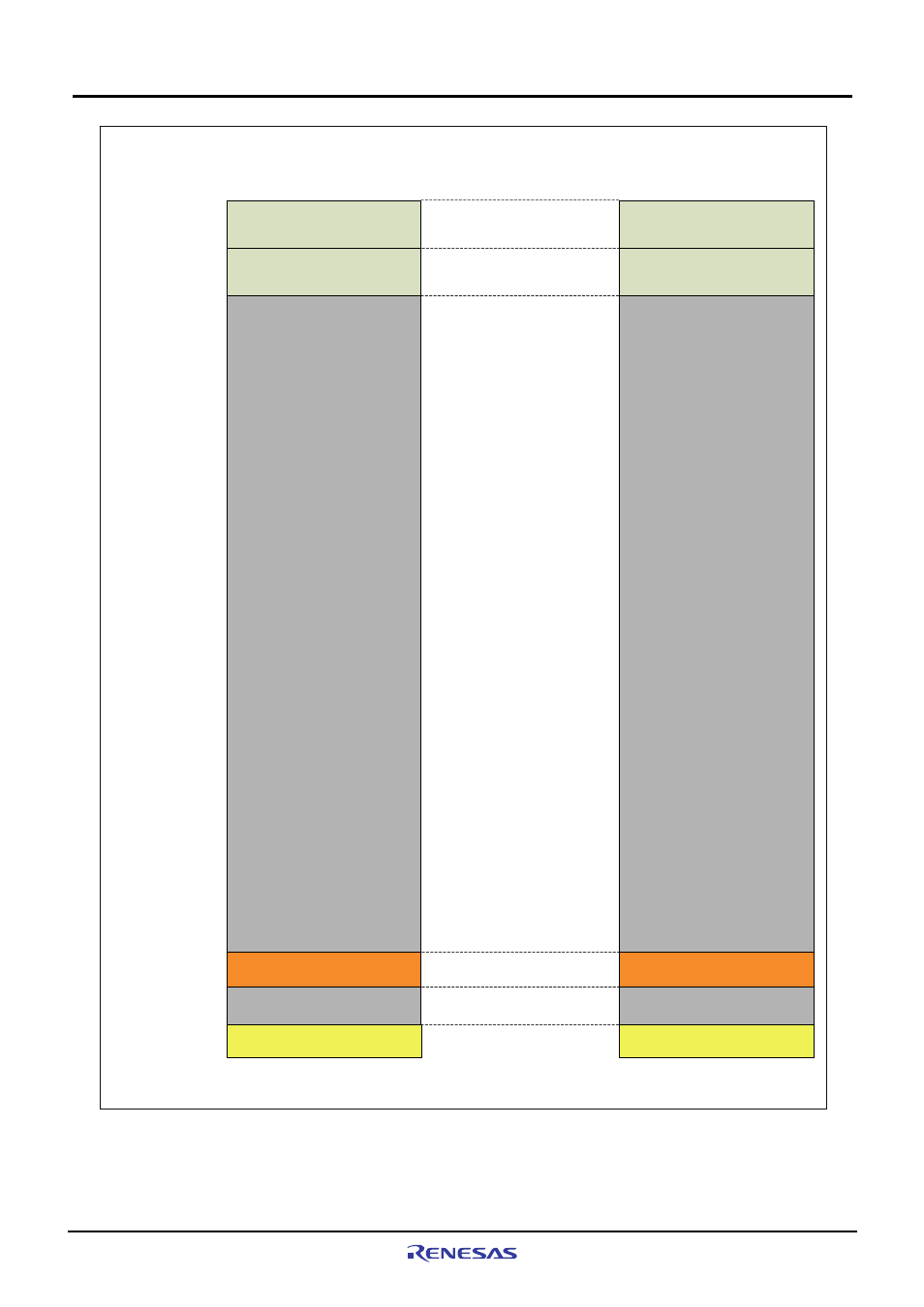
1.7 M3A-HS49 Memory Mapping
Rev.1.0 Dec 15, 2006
1-9
REJ10J0917-0100
1
CS0 space:64MB
CS1 space:64MB
Reserved
Logical space of the SH7149
MCU mode 0,1
(On-chip ROM disabled mode)
On-chip RAM(8KB)
On-chip Peripheral Module
H’0000 0000
H’03FF FFFF
H’0400 0000
H’07FF FFFF
H’0800 0000
H’FFFF 8FFF
H’FFFF 9000
H’FFFF AFFF
H’FFFF B000
H’FFFF BFFF
H’FFFF C000
H’FFFF FFFF
User Area
*
User Area
*
Memory Mapping
of the M3A-HS49
予約領域
(使用禁止)
Reserved
On-chip RAM(8KB)
On-chip Peripheral Module
H’0000 0000
Reserved
Reserved
H’03FF FFFF
H’0400 0000
H’07FF FFFF
H’0800 0000
H’FFFF 8FFF
H’FFFF 9000
H’FFFF AFFF
H’FFFF B000
H’FFFF BFFF
H’FFFF C000
H’FFFF FFFF
[Note]
*
:Because the address pins of SH7149 are A19 to A0, the address space that can be actually used is 1MB.
Figure1.7.2 Memory Mapping Example of SH7149 (MCU mode 0,1)