Overview – Renesas SH7149 User Manual
Page 16
Overview
1.7 M3A-HS49 Memory Mapping
Rev.1.0 Dec 15, 2006
1-10
REJ10J0917-0100
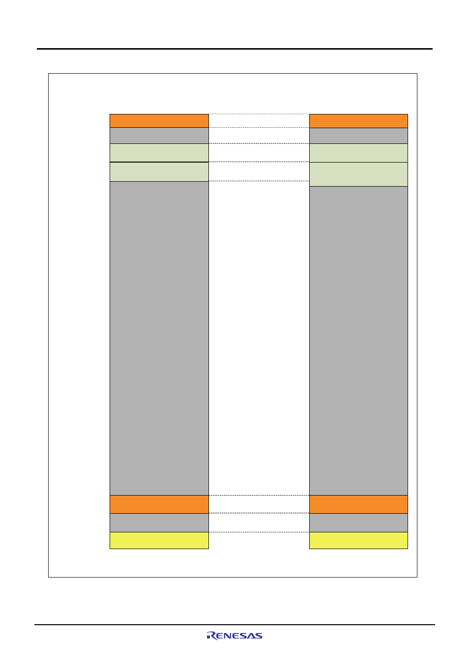
1
On-chip ROM(256KB)
CS1 space:64MB
Reserved
Logical space of the SH7149
MCU mode 2
(On-chip ROM enabled mode)
On-chip RAM(8KB)
On-chip Peripheral Module
H’0000 0000
H’03FF FFFF
H’0400 0000
H’07FF FFFF
H’0800 0000
H’FFFF 8FFF
H’FFFF 9000
H’FFFF AFFF
H’FFFF B000
H’FFFF BFFF
H’FFFF C000
H’FFFF FFFF
Memory Mapping
of the M3A-HS49
Reserved
On-chip RAM(8KB)
On-chip Peripheral Module
Reserved
Reserved
H’FFFF 8FFF
H’FFFF 9000
H’FFFF AFFF
H’FFFF B000
H’FFFF BFFF
H’FFFF C000
H’FFFF FFFF
CS0 space:64MB
H’0003 FFFF
H’0004 0000
H’01FF FFFF
H’0200 0000
Reserved
H’0000 0000
H’03FF FFFF
H’0400 0000
H’07FF FFFF
H’0800 0000
H’0003 FFFF
H’0004 0000
H’01FF FFFF
H’0200 0000
On-chip ROM(256KB)
User Area
*
User Area
*
Reserved
[Note]
*
:Because the address pins of SH7149 are A19 to A0, the address space that can be actually used is 1MB.
Figure1.7.3 Memory Mapping Example of SH7149 (MCU mode 2)