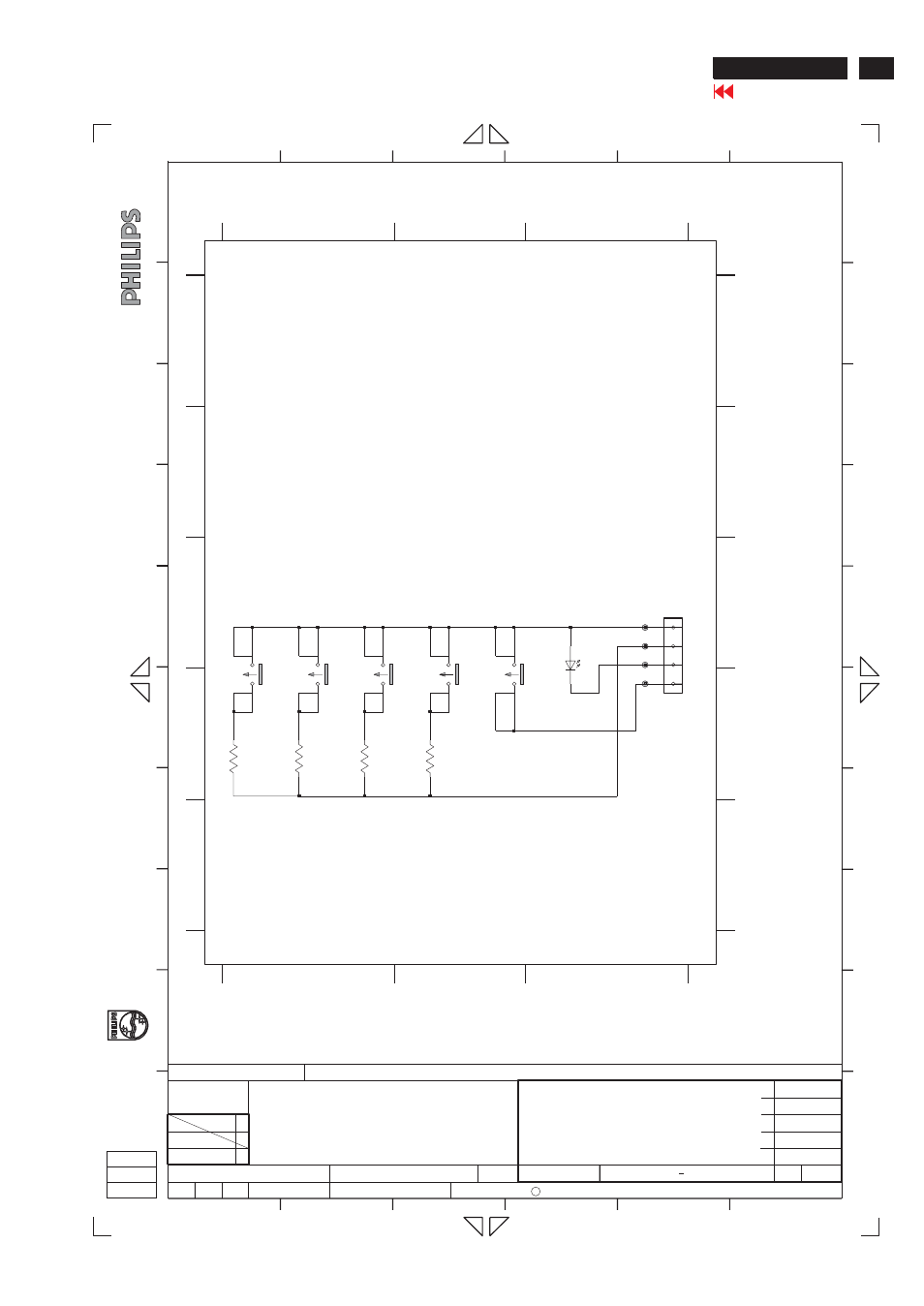
Schematic diagram of control board, A2 j, Ih g f e – Philips V30 User Manual
Page 37: Control pcb, De b
X
Go to cover page
37
107T5
Schematic Diagram of Control board
C
Left
A
2
J
1894 D2
1895 D3
3891 D1
3892 D1
4
3
4
5
6
I
1/2W
I
H
G
F
E
F4 D3
1891 D1
3
1/2W
1/2W
1/2W
OK
Right
CONTROL PCB
SB: 57231 x1
PB: 57271
T
O
MAIN
BD
1803
Alle
rechten
voorbehouden.
V
erveelvuldiging,
geheel
of
A
B
C
D
E
1
gedeeltelijk,
is
niet
toegestaan
dan
met
schriftelijke
3893 D1
3894 D2
6891 C3
8899 C3
D
E
B
is
prohibited
without
the
written
consent
of
the
copyright
1
POWER
LF
1892 D1
1893 D2
All
rights
reserved.
Reproduction
in
whole
or
in
parts
toestemming
van
de
auteursrechthebbende.
J
H
A
B
C
D
E
F1 C3
F2 C3
F3 C3
[R] STANDS FOR COMPONENT RESERVED.
2
1
6
5
F4
1%
1%
1%
1%
2
3
1
2
3
A
B
C
F
G
D
C
owner
.
F3
3
F1
F2
CONTROL BOARD
107T51/00
3138 178 6374
CHECK
DATE
NAME
1
SUPERS.
CLASS_NO
CHN
SETNAME
V30
1
1
2003-01-03
KONINKLIJKE PHILIPS ELECTRONICS N.V. 2000
2003-01-03
TYT12-
Roland/Ivy Su
2003-01-03
2
3
4
130
A4
1
2
3
4
1894
1
L-34GD
6891
8899
JFE3309V
4
1892
1
2
3
4
1893
1
2
3
3891
12K
3893
47K
3892
18K
1
2
3
4
3894
100K
1895
1
2
3
4
1891
- 150B (22 pages)
- 220SW9FS (118 pages)
- 1.09E+52 (2 pages)
- 109S (108 pages)
- 107P50 (2 pages)
- 150b5 (87 pages)
- 109B4x (2 pages)
- 107G (94 pages)
- 109B60 (2 pages)
- 150B3M/150B3Q (89 pages)
- 107T60 (2 pages)
- 107T70 (3 pages)
- 220VW8 (92 pages)
- 220VW8 (86 pages)
- 220VW8 (60 pages)
- 200WS8 (89 pages)
- 190C6 (95 pages)
- SVGA/EVGA 15C04204 (16 pages)
- 107B75 (2 pages)
- 107S76 (3 pages)
- VSS9451 (6 pages)
- 150B6CG (2 pages)
- 109B72 (3 pages)
- 107E69 (46 pages)
- 109E51 (2 pages)
- 104S19 (2 pages)
- 107E (123 pages)
- 107S4 (101 pages)
- 150E6 (70 pages)
- 107E71/00 (2 pages)
- 107H62 (2 pages)
- 107S63 (46 pages)
- 107T40 (2 pages)
- 190C8 (112 pages)
- 190C8 (118 pages)
- 200XW7 (109 pages)
- 190TW8 (19 pages)
- 107X2 (145 pages)
- 150C5BS (2 pages)
- 107B5 (137 pages)
- 105E (56 pages)
- 105E (54 pages)
- 150B (81 pages)
- 150P2M (89 pages)
- 170X6 (97 pages)