Controller board – Siemens SED2 VFD Electronic Bypass Option 125-3208 User Manual
Page 13
Electronic Bypass Option Overview
Siemens Building Technologies, Inc.
5
Controller Board
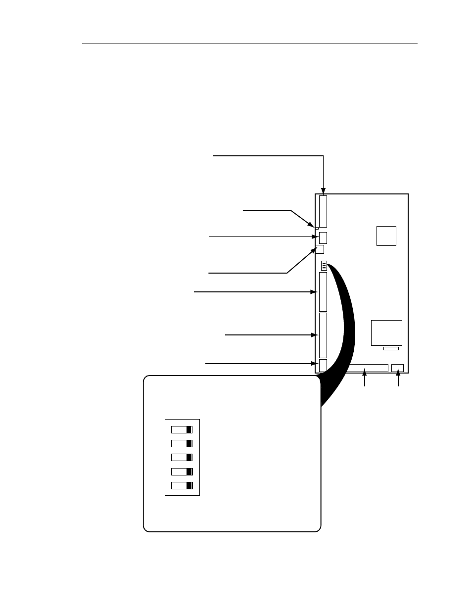
The Controller board is the foundation of the SED2 Electronic Bypass Option. It
controls communications to and from the SED2, keypad, isolated digital inputs,
relay/digital outputs, and contactors (Figure 3).
CONTACTOR
CONTROLS
POWER
OVERRIDE JUMPER
Supports six digital relay outputs for customer use.
Each relay has a maximum rating of 2A at 120 Vac.
Supports six isolated digital inputs for customer use.
The inputs require a contact closure capable of
providing a low impedance path at currents less
than 20 mA.
Supports inputs and outputs from the Electronic
Bypass Option keypad. The keypad provides
user interface indicators and push buttons.
Supports two SED2 non-isolated, digital relay
outputs and three SED2 digital inputs. The
maximum current draw for a relay output is 2 mA and
the voltage between the digital output source and return
lines is 24V. The Controller board provides unregulated,
non-isolated 24V to power the SED2 digital inputs.
Provides indication of initialization and
normal operation.
Connector J8 is for factory use only.
DIGITAL RELAY OUTPUTS
DIGITAL INPUTS
KEYPAD INTERFACE
SED2 INTERFACE
BASIC SANITY TEST INDICATOR
FACTORY USE ONLY
DIP SWITCHES
The Controller board DIP switches enable/disable
the Electronic Bypass Option features.
ON
12
5
34
OPTIONS
OFF
ON
SW1
12
5
34
Not used, factory test selector switch #2;
leave this switch OFF.
Interlock selector switch; requires
SED2 programming.
Automatic Bypass selector switch;
requires SED2 programming.
Essential Services selector switch.
Not used, factory test selector switch #1;
leave this switch OFF.
When the switch is ON the option is enabled;
when the switch is OFF the option is disabled.
J4
J5
J7
ON
OFF
MCU
TRANSFORMER
CONTROLLER
BOARD
SW1
F1
J3
J8
J2
J1
J6
VFD0095R1
Figure 3. Controller Board Inputs and Outputs.