Block diagram – Intel GA-G1975X User Manual
Page 8
- 8 -
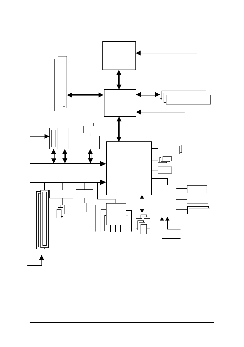
Block Diagram
(Note 1) DDR II memory can be overclocked to 888MHz (must be used with a 1066MHz FSB processor)
through overclocking in BIOS. Go to GIGABYTE's website for more information about the
supported DDR II memory modules for this feature.
(Note 2) To use a DDR II 667 memory module on the motherboard, you must install an 800/1066MHz
FSB processor.
LGA775
Processor
CPUCLK+/-(266/200 MHz)
PCI Express x16
Host
Interface
Intel
®
975X
MCHCLK (266/200MHz)
DDRII 888
(Note 1)
/ 667
(Note 2)
/
533MHz
DIMM
24MHz
33MHz
IT8712
ATA33/66/100
IDE Channel
Intel
®
ICH7R
Dual BIOS
2 PCI
PCI Bus
2 PCI Express x 4
PCI Express Bus
Dual Channel Memory
PS/2 KB/Mouse
COM Port
PCI-ECLK
(100MHz)
2 PCI-ECLK
(100MHz)
4 SATA 3Gb/s
Broadcom
5789
x 1
LAN1
RJ45
x4/x1
x4/x1
PCICLK(33MHz)
3 IEEE1394a
TSB43AB23
IT8211F
AT
A33 / 66 / 100 / 133 IDE Channel
8 USB
Ports
SPDIF Out
Center/Subwoofer Speaker Out
Line-Out
MIC
Line-In
SPDIF In
Side Speaker Out
Surround Speaker Out
CREATIVE
CA0106
Floppy
- 41210 (64 pages)
- 8xC251TQ (20 pages)
- ENTERPRISE PRINTING SYSTEM (EPS) 4127 (84 pages)
- U3-1L (20 pages)
- 80960HA (104 pages)
- X58 (54 pages)
- ESM-2850 2047285001R (91 pages)
- ATOM US15W (54 pages)
- D915GVWB (4 pages)
- XP-P5CM-GL (28 pages)
- AX965Q (81 pages)
- CORETM 2 DUO MOBILE 320028-001 (42 pages)
- CV700A (63 pages)
- 80C188EA (50 pages)
- X25-M (28 pages)
- XP-P5IM800GV (26 pages)
- IB868 (60 pages)
- D865GVHZ (88 pages)
- IB865 (64 pages)
- Altera P0424-ND (1 page)
- 8086-2 (30 pages)
- IXDP465 (22 pages)
- IWILL P4D (104 pages)
- GA-8I955X PRO (88 pages)
- FSB400 (PC2100) (96 pages)
- D845GLAD (4 pages)
- NAR-3041 (1 page)
- 87C196CA (136 pages)
- G52-M6734XD (74 pages)
- A96134-002 (10 pages)
- Express Routers 9000 (8 pages)
- 82540EP (45 pages)
- D865GLC (94 pages)
- IB850 (69 pages)
- MB898RF (62 pages)
- Arima LH500 (78 pages)
- V09 (33 pages)
- I/O Processor (22 pages)
- M600 (110 pages)
- SE7520JR2 (63 pages)
- SERVER BOARD S5520HCT (30 pages)
- Extensible Firmware Interface (1084 pages)
- GA-8IPXDR-E (70 pages)
- D845EBG2 (4 pages)
- AW8D (80 pages)