Bandgap analog voltage filter circuit – Intel 41210 User Manual
Page 52
52
Intel® 41210 Serial to Parallel PCI Bridge Design Guide
Circuit Implementations
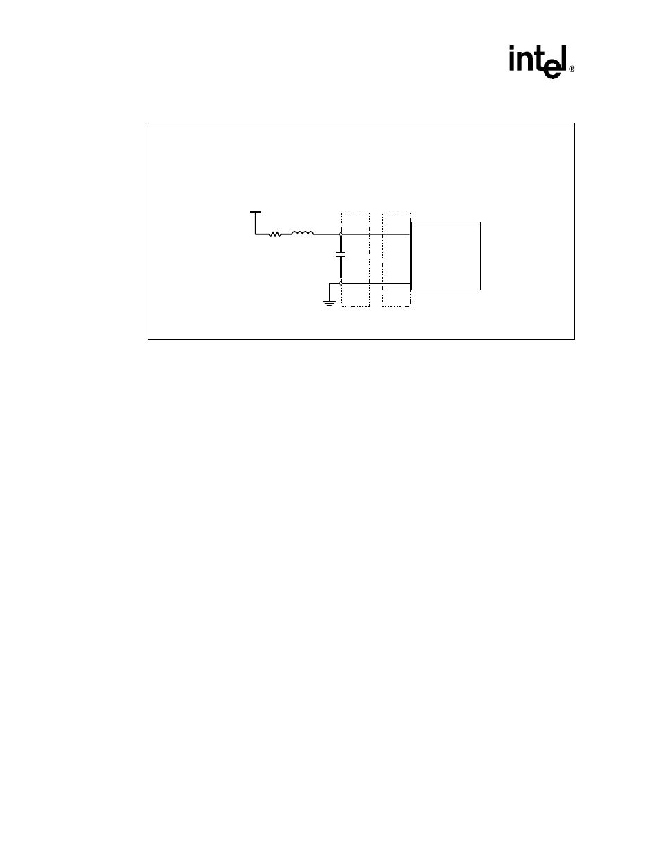
Figure 25.
Bandgap Analog Voltage Filter Circuit
Note:
.
•
Place C as close as possible to package pin.
•
R must be placed between the 2.5V supply and L.
•
Route VCCBGPE and VSSBGPE as differential traces.
•
VCCBGPE and VSSBGPE traces must be ground referenced (No 2.5V references).
•
VSSBGPE should be grounded at the capacitor.
•
Max total board trace length = 1.2”.
•
Min trace space to other nets = 30 mils.
B2726 -01
R
C
VSSBGPE
Note: Ground VSSBGPE at capacitor
VSS
Intel
fi
41210
Bridge
VCCBGPE
L
2.5 V
Board Trace:
Trace Width > 25 mils
Trace Spacing < 10 mils
Trace Length < 600 mils
Breakout Trace:
Trace Width > 6 mils
Trace Spacing < 6 mils
Trace Length < 600 mils
Board Route
Traces
Breakout
Traces
- 8xC251TQ (20 pages)
- ENTERPRISE PRINTING SYSTEM (EPS) 4127 (84 pages)
- U3-1L (20 pages)
- 80960HA (104 pages)
- X58 (54 pages)
- ESM-2850 2047285001R (91 pages)
- ATOM US15W (54 pages)
- D915GVWB (4 pages)
- XP-P5CM-GL (28 pages)
- AX965Q (81 pages)
- CORETM 2 DUO MOBILE 320028-001 (42 pages)
- CV700A (63 pages)
- 80C188EA (50 pages)
- X25-M (28 pages)
- XP-P5IM800GV (26 pages)
- IB868 (60 pages)
- D865GVHZ (88 pages)
- IB865 (64 pages)
- Altera P0424-ND (1 page)
- 8086-2 (30 pages)
- IXDP465 (22 pages)
- IWILL P4D (104 pages)
- GA-8I955X PRO (88 pages)
- FSB400 (PC2100) (96 pages)
- D845GLAD (4 pages)
- NAR-3041 (1 page)
- 87C196CA (136 pages)
- G52-M6734XD (74 pages)
- A96134-002 (10 pages)
- Express Routers 9000 (8 pages)
- 82540EP (45 pages)
- D865GLC (94 pages)
- IB850 (69 pages)
- MB898RF (62 pages)
- Arima LH500 (78 pages)
- V09 (33 pages)
- I/O Processor (22 pages)
- M600 (110 pages)
- SE7520JR2 (63 pages)
- SERVER BOARD S5520HCT (30 pages)
- Extensible Firmware Interface (1084 pages)
- GA-8IPXDR-E (70 pages)
- D845EBG2 (4 pages)
- AW8D (80 pages)