1 pci resistor compensation, 3 pci general layout guidelines, Pci resistor compensation – Intel 41210 User Manual
Page 33: Pci general layout guidelines, Pci rcomp
Intel® 41210 Serial to Parallel PCI Bridge Design Guide
33
PCI-X Layout Guidelines
•
Priority group for a master (i.e., whether a master is in low priority group or high priority
group).
•
Bus parking on last PCI agent or the bridge.
By default the arbiter parks the bus on the bridge and drives the A/D, C/BE# and PAR lines to a
known value while the bus is idle.
8.2.1
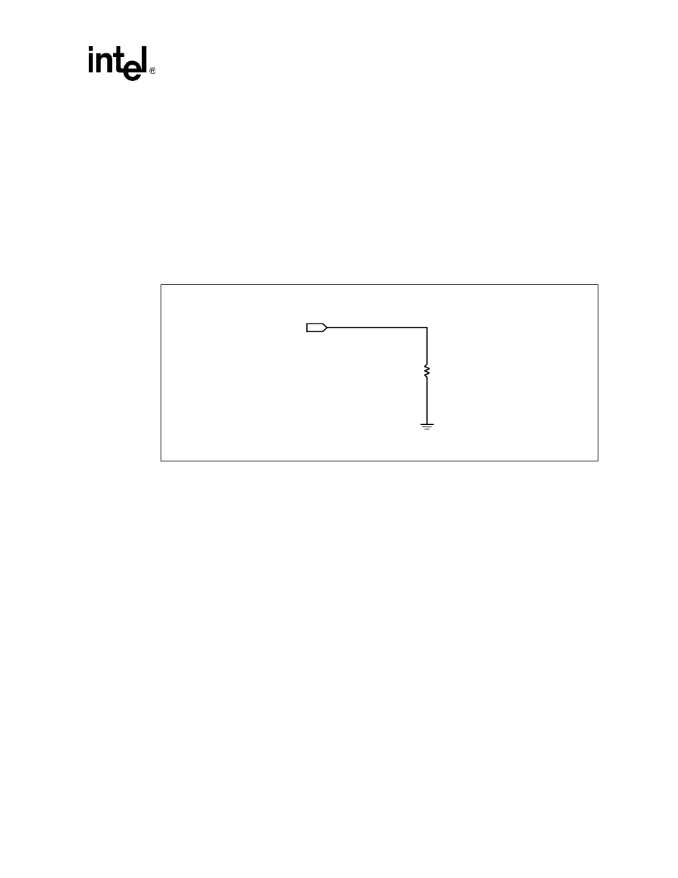
PCI Resistor Compensation
provides the recommended resistor compensation pin termination for the PCI A and PCI
B buses.
8.3
PCI General Layout Guidelines
For acceptable signal integrity with bus speeds up to 133 MHz it is important to PCB design layout
to have controlled impedance.
•
Signal traces should have an unloaded impedance of 60 +/- 10%
Ω
.
•
Signal trace velocity should be roughly 150 – 190 ps/inch
There are a couple of general guidelines which should be used when routing your PCI bus signals:
•
Avoid routing signals > 8”.
•
The following signals have no length restrictions: A_INTA#, A_INTB#, A_INTC#,
A_INTD#, B_INTA#, B_INTB#, B_INTC#, B_INTD# and TCK, TDI, TDO, TMS and
TRST#. Most PCI-X signals are timing critical. These signals have length restrictions for
propagation, setup, and hold requirements.
shows the PCI-X signals.
Figure 16. PCI RCOMP
B2718 -01
RCOMP
100
Ω
– 1%