Chapter 3, Motherboard information, Power switch through phoenix contact(j12) – Lanner LEC-7100 User Manual
Page 14
11
Motherboard Information
Chapter 3
Embedded and Industrial Computing
M17
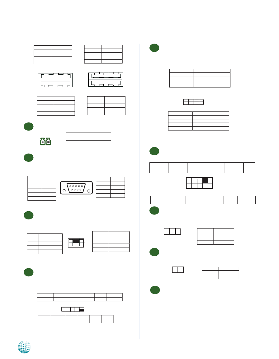
Power Switch through Phoenix Contact(J12)
M18
DIO Ports(CN14): The 8 pins of General Purpose Input/
Output (GPIO) can be can be configured as an either
input or output through the DB-9 female connector.
M19
PS/2 Keyboard & Mouse Connector (J9): It is for
connecting the PS/2 keyboard and mouse interface
cable.
M20
Dual USB Interface Connector (J10 for USB No.4 and
No.5): It is for connecting the USB module cable. It
complies with USB2.0 and support up to 480 Mbps
connection speed.
M21
Miscellaneous Pin Header (J11): Theses pin headers
can be used as a backup for the following functions:
Harddisk LED, Reset Button, and Power LED indicator.
M22
Internal Audio Connector(J2): It is an redundant pin
header for connecting an audio interface cable.
M23
SM-Bus Reserved (J6): System Management Bus.
It can be connected to read the value of the CPU
register.
M24
Thermal Sensor Connector(J13): It is for connecting
a temperature monitor.
Mini-PCI Connector (at the back, CN19)
Pin No.
Pin Name
1
Input0
2
Input1
3
Input2
4
Input3
5
GND
Pin No.
Pin Name
6
Output0
7
Output1
8
Output2
9
Output3
9 8 7 6
5 4321
Pin No.
Pin Name
1
VCC
3
MSDATA
5
KBDATA
7
GND
Pin No.
Pin Name
2
MSCLK
4
KEY
6
KEY
8
KBCLK
2 4 6 8
1 3 5 7
PIN NO.
1
3
5
7
9
Function USB_VCC USBD4- USBD4+
GND
Function
USB_VCC
USBD5- USBD5+ GND
NC
PIN NO.
2
4
6
8
10
2 4 6 8 10
1 3 5 7 9
1 2
Pin No.
Function
1
1 PWR_BTN_N
2
GND
PIN NO.
LINE_OUT2_L
GND
MIC_OUT_L
GND
Function
2
4
6
8
10
Pin No.
1
3
5
7
9
Pin Name LINE_OUT2_R
GND
MIC_OUT_R
LINE_IN_R
LINE_IN_L
2 4 6 8 1 0
1 3 5 7 9
7 5 3 1
8 6 4 2
PIN No.
Function
2
PWDLED
4
PWROK_100MS_N
6
FP_PWR_BTN_N
8
GND
PIN No.
Function
1
HardDisk LED
3
HardDisk_LED_N
5
FP_RST_BTN_N
7
GND
1 2
Pin No.
Pin Name
1
System_temp
2
GND
1 2 3
Pin No.
Pin Name
1
Smbdata
2
GND
3
SmbCLK
Pin No.
Function
1
USB_VCC
2
USBD0-
3
USBD0+
4
GND
Pin No.
Function
5
USB_VCC
6
USBD1-
7
USBD1+
8
GND
1 2 3 4
5 6 7 8
Pin No.
Function
1
USB_VCC
2
USBD2-
3
USBD2+
4
GND
Pin No.
Function
5
USB_VCC
6
USBD3-
7
USBD3+
8
GND
1 2 3 4
5 6 7 8
M25