Chapter 3, Motherboard information – Lanner LEC-7100 User Manual
Page 13
10
Motherboard Information
Chapter 3
Embedded and Industrial Computing
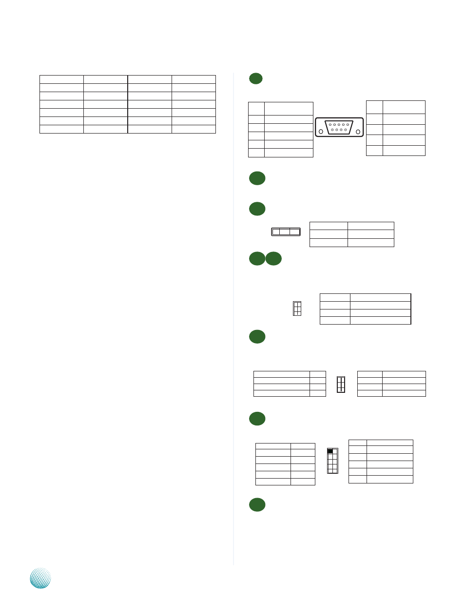
M9
RS-232 COM Port(COM1, CN18): It is the RS-232 serial
port.
M10
SO-DIMM Socket (CN8): It is for connecting the DDR2
667 (200 pin) memory. The system can suport up to 2
GB in maximum.
M11
Clear CMOS jumper (JP3): It is for clearing the CMOS
memory.
M12 M14
Ring-indicator Jumper Setting (JP1, JP2): The
Ring indicator pinout of the RS-232 COM port (JP2 for
COM1 and JP1 for COM2) can be altered according to
the following jumper settings.
M13
Mini-PCIe Wireless LED(J7): It shows the wireless
connection status for wireless modules connected in
Mini-PCIe Socket.
M15
RS-232 COM Port(COM2, J8): It is for connecting the
RS-232 interface cable .
M16
USB Ports (No. 0/1/2/3): The system provides 4
external USB [CN16 for USB0, USB1 (the bottom one
is USB0; the upper one is USB1) and CN17 for USB2,
USB3 (the bottom one is USB2; the upper one is
USB3)] type A connectors.
Pin No.
Function
1-2
Normal (Default)
2-3
Clear CMOS
1 2 3
6
4
2
5
3
1
Pin No.
Function
5
LED1_WPAN_N
3
LED1_WLAN_N
1
LED1_WWAN_N
Function
Pin No.
LED1R_WPLAN_N
6
LED1R_WLAN_N
4
LED1R_WWAN_N
2
Pin No.
Function
1-2
Supply +5V to Device
3-4
Supply +12V to Device
5-6
RS-232 Ring
6
4
2
5
3
1
6 7 8 9
1 2 3 4 5
P i n
No.
Pin Name
1
Data Carrier Detectg
2
Receive Data
3
Transmit Data
4
Data Terminal Ready
5
Ground
P i n
No.
Pin Name
6
Data Set Ready
7
Request to Send
8
Clear to Send
9
Ring Indicator
Pin No.
Function
Key
10
Ring Indicator
8
Clear to Send
6
Request to Send
4
Data Set Ready
2
Pin No.
Function
9
Signal Ground
7
Data Terminal Ready
5
Transmitted Data
3
Received Data
1
Data Carrier Detected
10
8
6
4
2
9
7
5
3
1
39
Reserved
40
GND
41
Reserved
42
Reserved
43
Reserved
44
Reserved
45
Reserved
46
Reserved
47
Reserved
48
+1.5V
49
Reserved
50
GND
51
Reserved
52
+3.3V