Chapter 3: motherboard information, Block diagram, Chapter 3 – Lanner FW-7610 User Manual
Page 10: Motherboard information, Fw-7610
7
Motherboard Information
Chapter 3
Network Application Platforms
Chapter 3:
Motherboard Information
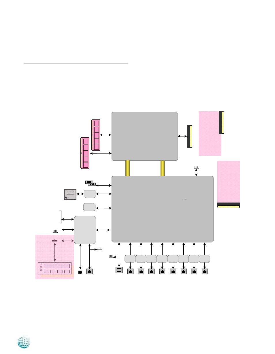
Block Diagram
The block diagram depicts the relationships among the
interfaces or modules on the motherboard. Please refer
to the following figure for your motherboard’s layout
design.
Intel Celeron Processor 827E
1.5M Cache, 1.40 GHz
Sandy Bridge
(FCBGA1023)
INTEL
HM65
LP
C
8x GbE RJ-45 / Connectors w/ LED
8x PCI-E x1
DDR3 MHz
ECC DIMM
Up to 16GB Maximum
2x 2.5" or
1x 3.5"
HD Bay
DMI2 x4
Compact
Flash
2x USB
PIN header
2x USB
connectors
USB 2.0
3x
SATA
II
D
ua
l
Ch
annels
PCI-E x8
Golden Finger
NUVOTON
NCT6776F
2x Console
PIN header
KB/Mouse
GPIO
Fan Monitor
Thermal Monitor
SPI
VGA
VGA PIN Header
For REAR DB19
RJ45
console
Watchdog
Reset
Bottom
By-pass
FW-7610
FDI
SPIF
223A
LCM
LCM Module
<
A
V
>
Intel
82574L
Intel
82574L
Intel
82574L
Intel
82574L
Intel
82574L
Intel
82574L
Intel
82574L
Intel
82574L
By-pass
(Optional)
(Optional)
RISER
To
Rear PCIE
(Optional)
RISER
For
Add-on
Front NIC
module