Functional description – Grass Valley 8950ADC User Manual
Page 39
8950ADC Instruction Manual
39
Functional Description
Functional Description
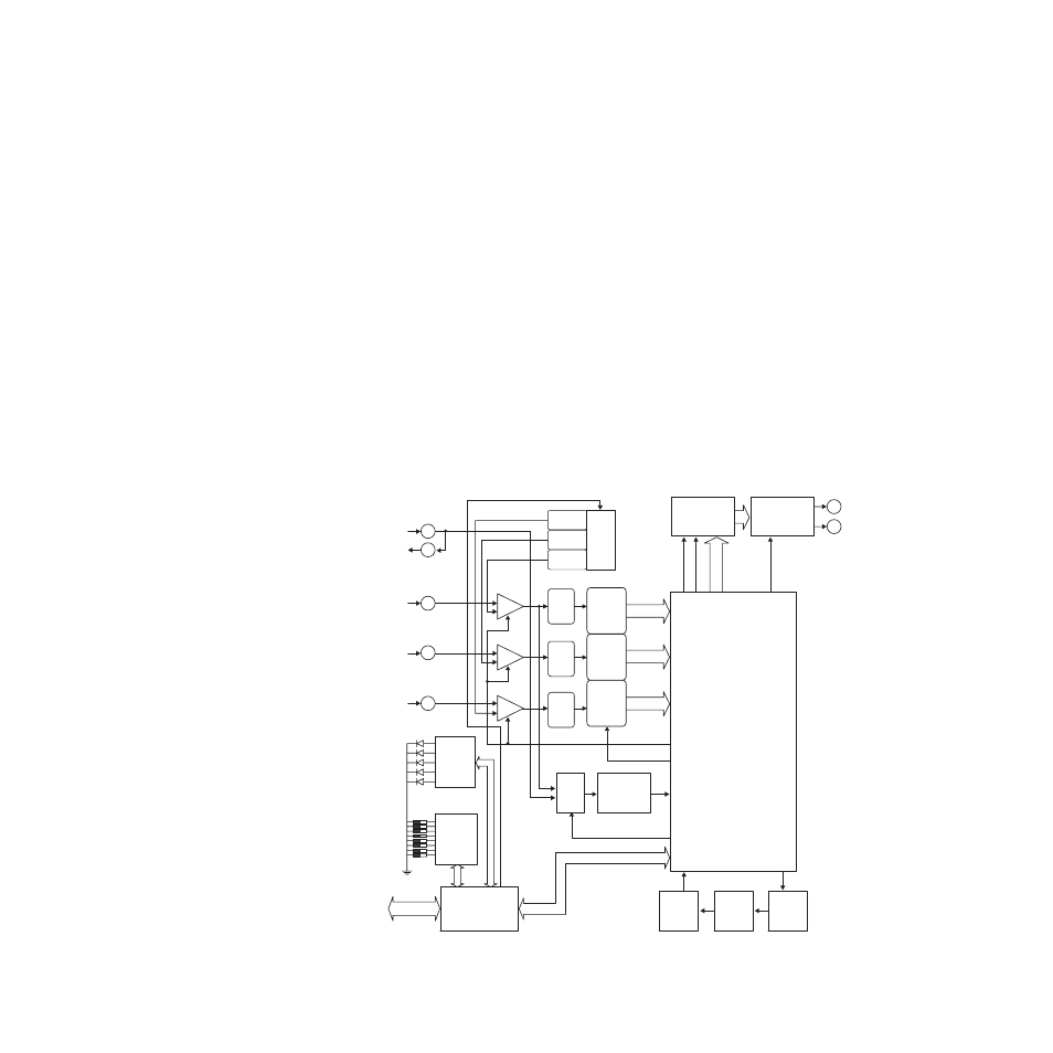
The 8950ADC converts an analog CAV or GBR video signal to the SMPTE
259M (270Mb/s) D1 serial component digital signal. The major functional
blocks are:
•
Input buffers, amplifiers and low pass filters (LPF)
•
Analog to digital converters (ADC)
•
Digital Signal Processing (DSP) Field Programmable Gate Array
(FPGA)
•
Digital to Analog Converters
•
Input Phase Lock Loop (PLL) and 54 MHz clock generator
•
Serializer
•
Delay line
•
Embedded processor
while reading the following func-
tional description.
Figure 18. 8950ADC Block Diagram
To Host
Sync
Separator
User
Setup
LEDs
LPF
LPF
LPF
Reference
Sync
Serial
Output
Y/G
(B-Y)/B
(R-Y)/R
10 bit+1
D1 Parallel
27 MHz
10 bit+1
10 bit+1
ADC
ADC
ADC
A
A
A
Parallel Interface
Reference Selection
54 MHz
Clamp
DAC
DAC
DAC
I2C
Inter-
face
Embedded
Processor
Mux
Loop
Filter
Phase
Comp.
Serializer
Delay Line
(2.5 max.)
VCXO
54 MHz
FPGA
Digital Signal
Processing
Timing
Sync Generator
Standard Detector
Filters
Color Space
Converter
0603_01