Figure 37: diamond channel hardware interface, Figure 38: node1 dsp sub-system, Smt6040 – Sundance SMT6040 User Manual
Page 44: Sundance simulink toolbox
Sundance Multiprocessor Technology Limited
Form : QCF32
SMT6040
“Sundance Simulink Toolbox”
Date : 6 July 2006
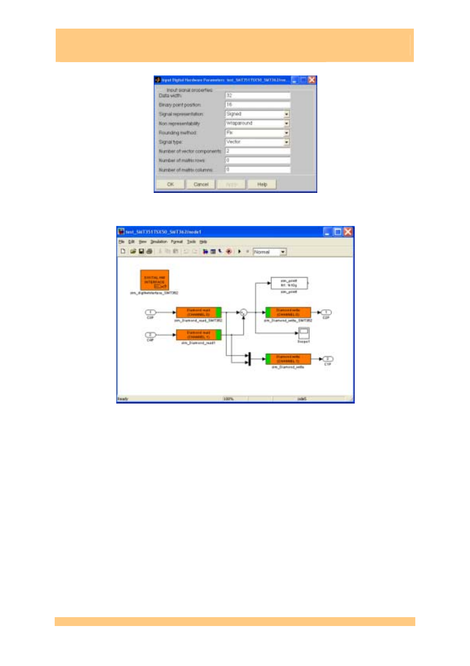
Figure 37: Diamond channel hardware interface
The second node (node1) is shown in Figure 38.
Figure 38: node1 DSP sub-system
It receives two sequences of data, from Diamond channel 0 (read) and Diamond channel 1
(read), respectively, which receive data from node root, as shown in the top diagram. These
are summed up together and the result is:
• Printed (sim_printf) to the console;
• Sent to the Diamond channel 0 (write), which is connected to the node root, as shown in
the top diagram;
• Muxed into a 2-elements vector and sent, via Diamond channel 1 (write) to the FPGA
module, as shown in the top diagram.
The sim_digHwInterface is exactly as in node root, as this is the second DSP of the same
SMT362 board.
The third node SMT350 implements the Simulink diagram that programs the FPGA +
ADC/DAC combination (in this example, SMT351T + SMT350 board). The SMT350
diagram is shown in Figure 39. This demonstrates how the SMT6040 can be used to program
FPGA modules and also to configure the SMT350 DAQ board.
SMT6040 - “Sundance Simulink Toolbox”
Last Edited: 08/01/2010 15.42
Page 44 of 53