Measurement Computing CIO-QUAD0x User Manual
Page 15
4.3 GLOBAL CONTROL REGISTERS (Base +8 through Base +12)
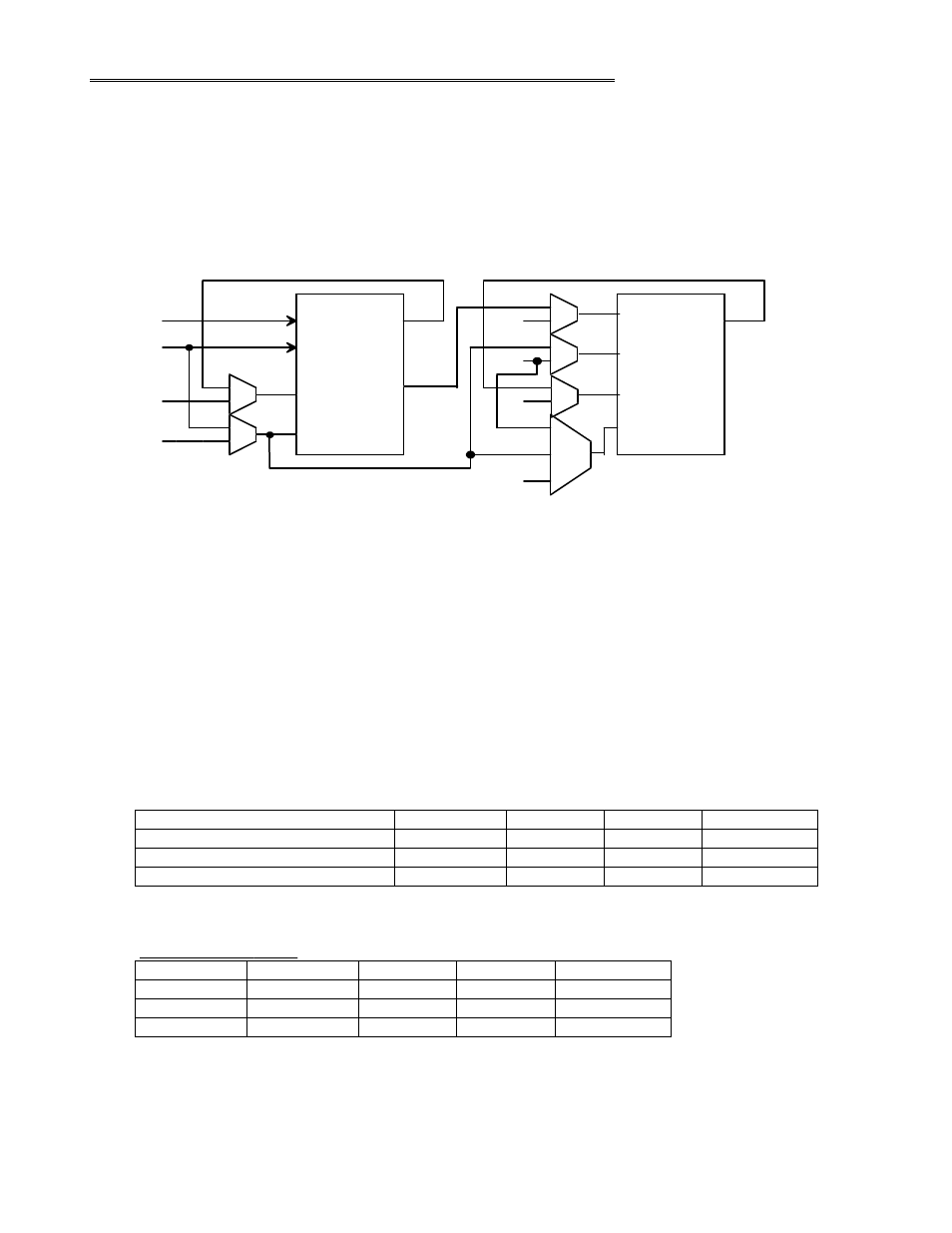
Five global control registers are located at offsets 8-12 from the base address. The following sections describe these five
registers and the various control functionalities which they provide. Unlike the channel configuration registers, the current
state of a global control register can be obtained through reading the register. To help understand these registers and
functions, refer to Figure 4-1, Counter Block Diagram as you read the register descriptions.
Counter Cascading Functional Diagram
1
0
1
0
1
0
1
0
1
0
00
01
10
1A
2A
2B
3A
3B
4A
4 B
1B
LS7266
LS7266
1A
1B
2A
2B
3A
3B
4A
4 B
PH2A
PH2B
PH3A
PH3B
PH4A
PH4AB1/B0
FLG1
FLG2
FLG3
FLG4
Figure 4-1. Counter Block Diagram
4.3.1 Base +8: Index & Interrupt Routing Control Register
The first four bits of this register route the index pin from the quadrature encoder to either the LCNTR/LOL input or the
RCNTR/ABG input for each of the four encoder inputs. The value set in this register should be consistent with the value
written in the IDR register. The most significant four bits select the interrupt source as either Compare select or
Carry/Borrow select.
The FLG1 and FLG2 output pins are register programmable for Carry, Borrow, Compare and flag status functions. The
COMPARE signal is actually the CARRY pin set to be the COMPARE flag through register IOR. (See 7266 IOR register
for proper functionality).
Interrupt Routing:
Register Base + 8 D4-D7
1
1
1
1
FLG2 - Borrow / Up / Down
0
0
0
0
FLG1 - Carry / Compare / Index
CBINT4
CBINT3
CBINT2
CBINT1
Input
Chan 4
Chan 3
Chan 2
Chan 1
Index Routing: Connects the index input to the counter control input pin below.
Register Base + 8 D0-D3
1
1
1
1
LCNTR/LOL
0
0
0
0
RCNTR/ABG
IND4SEL
IND3SEL
IND2SEL
IND1SEL
Input
Chan 4
Chan 3
Chan 2
Chan 1
11