Measurement Computing CIO-QUAD0x User Manual
Page 12
Reset and Load Signal Decoders (RLD)
The RLD contains three user configurable fields. This register controls all of the reset options as well as the data transfer
options. The following sections describe each field in the RLD register and the various modes that can be set for operation.
The RLD register is used to reset the counter and the status flags and also to provide access to the error bit E, which is the
only means for resetting this flag once it is set.
RLD Reset Byte Pointer Field (bit 0 - LSB)
This field (D0 - see Table 4-1) is used to reset the byte pointer. The byte pointer is auto-incremented each time the Output
Latch (OL) register is read or the Preset Register (PR) is written to. The byte pointer must be reset prior to any access to the
24-bit counter register.
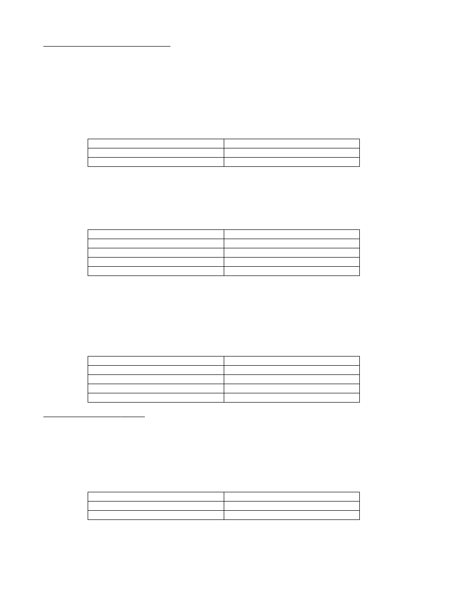
x00x xxx1
BP Reset
x00x xxx0
NOP
Bit 0 value for byte pointer reset
RLD Byte Pointer Reset
RLD Reset Fields (bits 1 & 2)
In addition to the byte pointer there are several other fields that can be reset. This field (D1 and D2 - see Table 4-1)
provides the mechanism for resetting the counter and all of the status flags. The Borrow Toggle (BT), Carry Toggle (CT),
Compare Toggle (CPT), and the Sign Flag (S) can all be reset through bits 1 and 2 of the RLD register. Finally, the only
way to clear the Error (E) flag after it has been set is through the RLD register.
x00x x11x
E
x00x x10x
BT, CT, CPT, and S
x00x x01x
CNTR
x00x x00x
NOP
Bit 1 & 2 value for reset fields
RLD Reset
RLD Transfer Fields (bits 3 & 4)
The final bit field in the RLD register consists of bits 3 and 4 (D3 and D4 - see Table 4-1). This field controls the data
transfer operation of the LS7266 chip. There are three options that are available as listed in the table below. The contents of
the Preset Register can be transferred to the Counter, the contents of the Counter can be copied to the Output Latch for
reading, and the Preset Register contents can be copied to the Filter Clock Prescalar. This register provides the software
mechanism for reading the current count from the encoder. First write to the RLD register to transfer the contents of the
counter to the output latch, then reset the byte pointer and perform three reads of the output latch.
x001 1xxx
Preset to Filter Clock Prescalar
x001 0xxx
Counter to Output Latch
x000 1xxx
Preset to Counter
x000 0xxx
NOP
Bit 3 & 4 value for transfer fields
RLD Transfer
Counter Mode Register (CMR)
The CMR contains three user-configurable fields, count representation, count mode, and quadrature scaling. Each field
consists of one or more bits in the CMR register. After you select the desired mode, assemble the bit fields into a byte that
can be written to the CMR register. Bits 5 and 6 are always (1) and (0), respectively, for CMR register accesses.
Data Encoding (bit 0 - LSB)
The quadrature count can be represented in either BCD or binary. Bit 0 (D0 - see Table 4-1) of the CMR register selects the
desired option.
x01x xxx1
BCD
x01x xxx0
BINARY
Bit 0 value for count configuration
CMR Count Representation
Count Mode (bits 1 & 2)
There are four different count modes that are selected by bits 1 and 2 (D1 and D2 - see Table 4-1). The count modes are;
Normal, Range-Limit, Non-recycle, and Modulo-N.
8