Measurement Computing CIO-DAS16/M1 User Manual
Page 22
18
A register stores the most recently written C/G memory address and this C/G element becomes the
RESTART ADDRESS. Each time the restart address is reached, the C/G address pointer is reset to point
to address 0, which contains the first element in the C/G list.
When the A/D starts the acquisition scan, the first sample is controlled from the first entry in the C/G
memory, address 0. The second sample is controlled by the second entry made in C/G memory and so on
until the RESTART ADDRESS (last entry) address of C/G memory is reached. At this point the C/G
memory pointer is reset to the address 0 and the sequence of C/G begins again. The process will repeat as
long as the A/D is acquiring data.
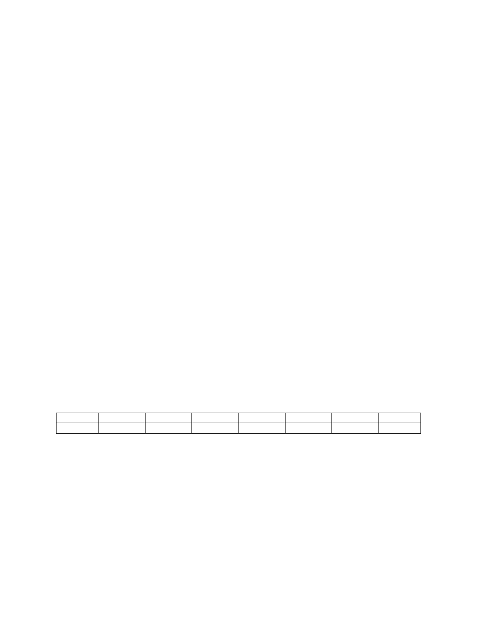
For the programmer who wants to write to the C/G memory directly, you must arrange the C/G scan as
follows:
Order to Execute
Channel/Gain
C/G Memory Address Pointer
First
3
0
Second
1
1
Third
2
2
Fourth
3
3
Fifth
4
4
Sixth (restart address) 5
5
NOTE: C/G data must be loaded into C/G memory in the order 0, 1, 2, 3, 4, 5 as in the example above.
TO LOAD THE C/G MEMORY:
1.) Write to Base + 6 to point to the C/G memory address,
2.) Write to Base + 7 to load the C/G data into the C/G memory address pointed to by Base + 6.
3.) Do this for each element in the C/G list.
4.) The last address written to the pointer, Base + 6, is the restart address.
NOTE: If you have loaded a long series of C/G entries into the C/G memory and you want to shorten the
list to use only the first N entries, simply re-write the Nth entry again. This updates the RESTART
ADDRESS in the restart address register.
NOTE: Any write to this register clears the FIFO buffer.
4.6.7
Channel Gain Queue Da ta Register
BASE ADDRESS + 7
7
6
5
4
3
2
1
0
RANGE
U/B
G1
G2
CH3
CH2
CH1
CH0
Range
Uni/Bip G1
G0
Input Range
Decimal Gain Code*
1
0
0
0
±10V
128
0
0
0
0
±5V
0
0
0
0
1
±2.5V
16
0
0
1
0
±1.25V
32
0
0
1
1
±0.625V
48
0
1
0
0
0 to10V
64
0
1
0
1
0 to 5V
80
0
1
1
0
0 to 2.5V
96
0
1
1
1
0 to 1.25V
112