Measurement Computing CIO-DAS16/M1 User Manual
Page 16
12
4.5
DT-CONNECT
The DT-Connect connector (P4) at the top of the CIO-DAS16/M1 board is included primarily for use
with the MEGA-FIFO huge sample buffer. Due to PC bus speed limitations and other transfer rate
degradations caused by Windows and other program overhead, it may be necessary to use the DT-
Connect and MEGA-FIFO. This allow you to take full advantage of the 1MHz A/D rate of the CIO-
DAS16/M1 regardless of other processes occuring simultaneously.
The CIO-DAS16/M1 DT-Connect is implemented in master mode only and must be the only DT-Connect
master in a system.
DT-Connect is an industry standard for board interconnect. The full standard is available for those
wishing to develop specialized DT-Connect accessories. The CIO-DAS16/M1 DT-Connect interface is a
standard implementation and so will operate with any DT-Connect compliant slave such as array
processors or DSP boards.
To use the DT-Connect, simply connect the CIO-DAS16/M1 with the slave board (MEGA-FIFO) via the
cable supplied with the slave. From that point on, all DT-Connect functions are under software control.
Measurement Computing’s Universal Library supports the CIO-DAS16/M1 DT-Connect interface with
the MEGA-FIFO and with any other slave board. DT-Connect slaves not supplied by Measurement
Computing will require software supplied by the manufacturer to manipulate or transfer the data
transferred to the slave by the CIO-DAS16/M1.
4.6
CONTROL & DATA REGISTERS
The CIO-DAS16/M1 is controlled and monitored by writing and reading from one 16-bit address at
BASE + 0 and then 14 consecutive 8-bit I/O addresses beginning at BASE + 2. The first address, or
BASE ADDRESS, is determined by setting a bank of switches on the board.
Usually, register manipulation is best done with ASSEMBLY language programs as most of the CIO-
DAS16/M1 possible functions are implemented in easy-to-use Universal Library routines callable from
Basic, PASCAL, C and FORTRAN libraries.
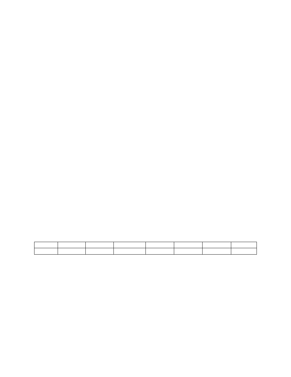
The register descriptions follow the format:
7
6
5
4
3
2
1
0
A/D9
A/D10
A/D11
A/D12 LSB
CH8
CH4
CH2
CH1
Where the numbers along the top row are the bit positions within the 8-bit byte and the numbers and
symbols in the bottom row are the functions associated with that bit.
To write to or read from a register in decimal or HEX, the bit weights in Table 4-2 apply.