Measurement Computing CIO-DAS16/M1 User Manual
Page 15
11
For the programmer who wants to write to the C/G memory directly, this means that you must arrange the
C/G scan as follows:
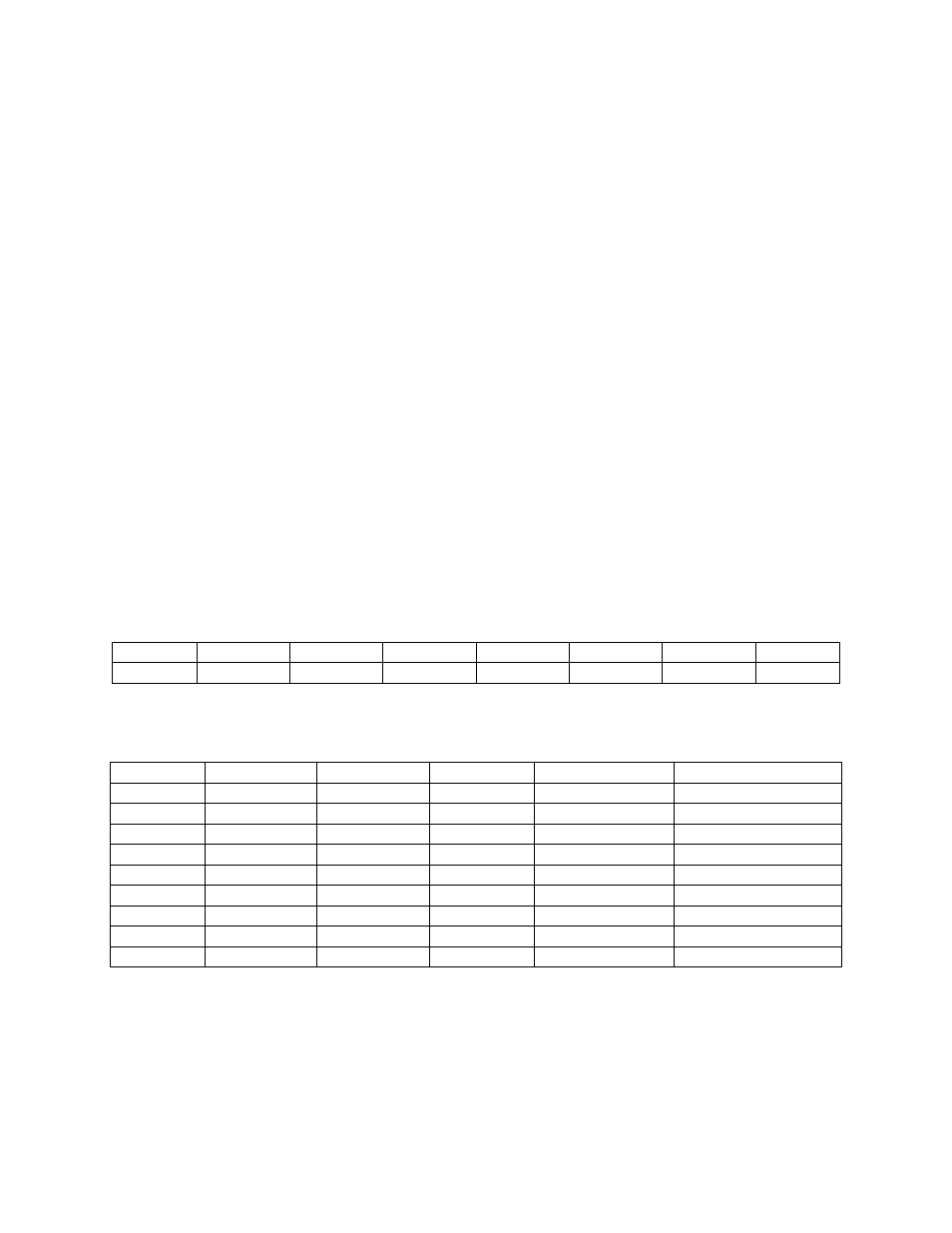
Order to Execute
Channel/Gain
C/G Memory Address Pointer
First
3
0
Second
1
1
Third
2
2
Fourth
3
3
Fifth
4
4
Sixth (restart address)
5
5
Note that the C/G data must be loaded into C/G memory in the order 0, 1, 2, 3, 4, 5 in the example above.
To load the C/G memory:
1. Write to Base + 6 to point to the C/G memory address,
2. Write to Base + 7 to load the C/G data into the C/G memory address pointed to by Base + 6.
3. Do this for each element in the C/G list.
4. The last address written to the pointer, Base + 6, is the restart address.
NOTE: If you have loaded a long series of C/G entries into the C/G memory and you want to shorten the
list to use only the first n entries, simply re-write the nth entry again. This updates the RESTART
ADDRESS in the restart address register.
NOTE: Any write to this register clears the FIFO buffer.
4.4
CHANNEL/GAIN MEMORY CONTENTS REGISTER
7
6
5
4
3
2
2
0
RANGE
U/B
G1
G0
SPARE
CH2
CH1
CH0
SPARE: Always write a “0” to this bit.
Table 4-1. Range/Mode Gain Codes
Range
Uni/Bip
G1
G0
Input Range
Decimal Gain Code
1
0
0
0
±10V
128
0
0
0
0
±5V
0
0
0
0
1
±2.5V
16
0
0
1
0
±1.25V
32
0
0
1
1
±0.625V
48
0
1
0
0
0 to 10V
64
0
1
0
1
0 to 5V
80
0
1
1
0
0 to 2.5V
96
0
1
1
1
0 to 1.25V
112
Decimal codes are for upper four bits only. In other words, this is the correct byte to write if the channel
is equal to zero. Channel values can be 0 to 15 (single ended) or 0 to 8 (differential) The code to write an
input range of ±2.5V on channel 7 would be 16 + 7 = 23.