Fluke Biomedical 956A-201-M2 User Manual
Page 58
3-32
Read-Write Cycles
A read cycle is performed by sequencing /RAM 0000 and /RAM READ, while /RAM WRITE is held high
(inactive). The address (A00 - A12) are latched by the failing edge of /RAM 0000. Data becomes valid
approximately 250 ns later.
A write cycle is performed by sequencing /RAM 0000 and /RAM WRITE, while holding /RAM READ high
(inactive). Identical to the read cycle, the address (A00 - A12) are latched by the falling edge of /RAM
0000. Data is stored into RAM on the failing edge of /RAM WRITE.
Write Register Decoding
Decoding for write registers within the main circuit board is performed by U2, which is a 1 of 8 decoder.
Control signals for U2 are /REGSELECT, /WRITE02, and /R/W (active high), as well as addresses A01,
A02, and A03. U2 decodes two addresses per output, starting at 4000, and ending with 400E. These
outputs are active low. Table 3-11 lists the write register assigned functions and addresses.
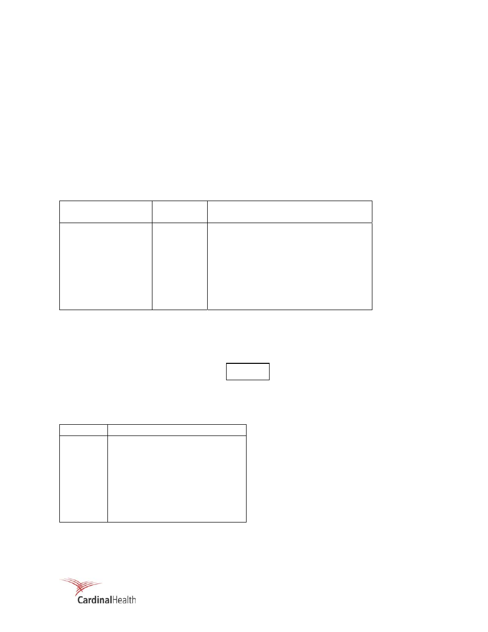
Table 3-11. Write Register Functions
ADDRESS STATE
A3 A2 A1
HEX
ADDRESS
FUNCTION
0 0 0 4000 Status
Indicators (/STATUS INDICATORS)
0 0 1 4002 E
2
PROM (/EEPROM)
0
1
0
4004
D/A Converter (/DAC)
0
1
1
4006
Display Control (/DISP. CONTROL)
1
0
0
4008
Display Data (/DISP. DATA)
1
0
1
400A
Counter Control (/COUNTER CONTROL)
1
1
0
400C
Relay Control (/400E)
1 1 1 400E
(Spare)
Counter Control (Write Only)
The counter control register (U43) is an 8-bit register with clear, and responds to address 400A. Upon
initial power-up (/RESET), the system reset signal sets all outputs low. The /COUNTER CONTROL
initiates data transfer to the register. Table 3-12 lists the counter control register write functions.
NOTE
Data written into U43 remains at the outputs until a reset occurs
or new data is written.
Table 3-12. Counter Control Register Write Functions
DATA BIT FUNCTION
D0 Counter
Clear
D1 Counter
Enable
D2 HV
Shutdown
D3 HV
Select
D4
Clear Switch Latch
D5 Not
Used
D6 Not
Used
D7 Not
Used
NOTE