Profibus dp slave communication module dvppf02-h2, 3 communication – Delta Electronics DVPPF02-H2 User Manual
Page 8
PROFIBUS DP Slave Communication Module DVPPF02-H2
DVP-PLC Application Manual
6
2.6 Installation
&
Wiring
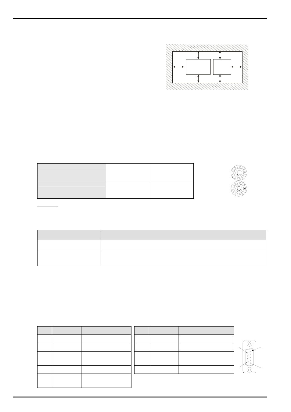
1. Install DVPPF02-H2 in an enclosure with sufficient
space around it to allow heat dissipation (see the
figure).
2.
DO NOT place the I/O signal wires and power supply
wire in the same wiring circuit.
D>50mm
PF02- H2
D
D
D
D
D
D
E 2 PLC
H
3 Communication
3.1 Address
Switch
The address switches are two rotary switches, x16
0
and x16
1
, setting up the node address of DVPPF02-H2
on PROFIBUS DP network. Rotate the switch to a position to indicate the value of the switch. The range for
each switch is 0 ~ F. The address switches are in hexadecimal form. The factor of x16
0
is 16
0
, and the factor of
x16
1
is 16
1
. The set value of the address switch is the sum of the value of each of the two switches multiplied
by its factor.
Value of address switch
Value at x16
1
Value at x16
0
Factor of address switch
16
1
16
0
NO
DE
ADD
R
ES
S
x16
0
x16
1
Example: If you need to set the node address of DVPPF02-H2 to “26” (decimal), simply switch x16
1
to “1”
and x16
0
to “A”. 26 (decimal) = 1A (hex) = 1 × 16
1
+ A × 16
0
.
Range for address switch:
Switch setting
Explanation
H’1 ~ H’7D
Valid PROFIBUS DP address
H’0 or H’7E ~ H’FF
Invalid PROFIBUS DP address
If the node address in within this range, NET LED will flash quickly in red.
Note:
z Please set up the node address when the power is switched off. After the setup is completed, re-power
DVPPF02-H2.
z When DVPPF02-H2 is operating, changing the set value of the node address will be invalid.
z Use slotted screwdriver to rotate the switch carefully in case you scratch the switch.
3.2
PROFIBUS DP Connection Port
PIN
PIN name
Definition
PIN
PIN name
Definition
1
--
N/C
6
VP
Power voltage – positive
2 --
N/C
7 --
N/C
3 RxD/TxD-P
Sending/receiving
data P(B)
8 RxD/TxD-N
Sending/receiving data
N(A)
4 --
N/C
9 --
N/C
5 DGND
Data reference
potential (C)
1
5
9
6