Ssram – Altera Cyclone III FPGA Starter Board User Manual
Page 25
Altera Corporation
2–17
April 2012
Cyclone III FPGA Starter Board Reference Manual
Board Components and Interfaces
SSRAM
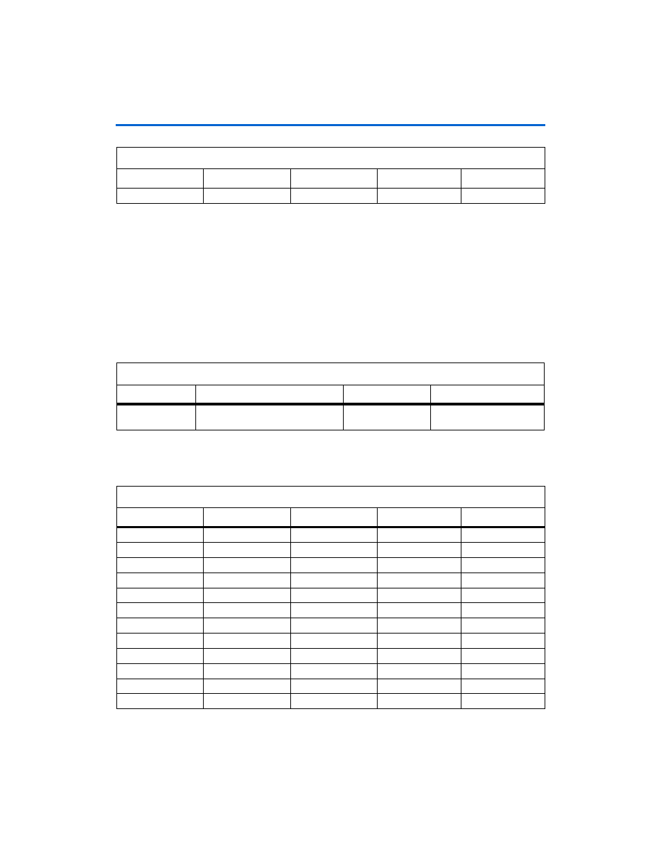
The Cyclone III FPGA starter board has a 256K x 32 synchronous SRAM.
Table 2–15
lists SSRAM board reference and manufacturing
information.
Table 2–16
shows the SSRAM signal name, corresponding FPGA pin,
signal direction, type, and board reference U5 SSRAM pin.
ddr_dq15
V14 Bidirectional
SSTL-2
65
Note to
Table 2–14
:
(1)
The Cyclone III EP3C25F324 only supports one I/O standard in an I/O bank. I/O banks 3 and 4 are shared among
the DDR, HSMC and LEDs. In several DDR designs, some of the I/O pins that share the same banks with the DDR
are unavailable for use due to different I/O standards. Therefore, if you have added DDR to your system, I/O
banks 3 and 4 is to be configured as SSTL-2 only while the HSMC and LEDs pins which are not using SSTL-2,
should be removed.
Table 2–14. DDR SDRAM Pinout (Part 3 of 3)
Note (1)
Signal Name
FPGA Pin
Direction
Type
U4 (DDR) Pin
Table 2–15. SSRAM Manufacturing Information
Board Reference
Description
Manufacturer
Manufacturer Part Number
U5
256K x 32 synchronous SRAM
Integrated Silicon
Solutions, Inc.
IS61LPS25636A-200TQL1
Table 2–16. SSRAM Pinout (Part 1 of 3)
Signal Name
FPGA Pin
Direction
Type
U5 (SSRAM) Pin
flash_sram_a2
A16
Output
2.5 V
37
flash_sram_a3
B16 Output
2.5 V
36
flash_sram_a4
A15 Output
2.5 V
35
flash_sram_a5
B15 Output
2.5 V
34
flash_sram_a6
A14 Output
2.5 V
33
flash_sram_a7
B14 Output
2.5 V
32
flash_sram_a8
A13 Output
2.5 V
44
flash_sram_a9
B13 Output
2.5 V
45
flash_sram_a10
A12 Output
2.5 V
46
flash_sram_a11
B12 Output
2.5 V
47
flash_sram_a12
A11 Output
2.5 V
48
flash_sram_a13
B11 Output
2.5 V
49