Clocking circuitry, Clocking circuitry –6 – Altera Cyclone III FPGA Starter Board User Manual
Page 14
2–6
Altera Corporation
Cyclone III FPGA Starter Board Reference Manual
April 2012
Clocking Circuitry
Table 2–3
lists the Cyclone III EP3C25F324 device pin count.
You can configure the Cyclone III device via the on-board USB-Blaster
™
or
through the JTAG interface using an external programming cable (sold
separately).
f
For additional information about Altera devices, go to
.altera.com/products/devices
.
Clocking
Circuitry
The Cyclone III FPGA starter board’s clocking circuitry
is designed to be
simple and easy to use.
A single 50-MHz clock input is used and all other
clocks are generated using the Cyclone III device’s phase-locked loops
(PLLs). The dedicated PLLs are used to distribute the flash, SSRAM, and
HSMC clocks.
shows the clock pinout.
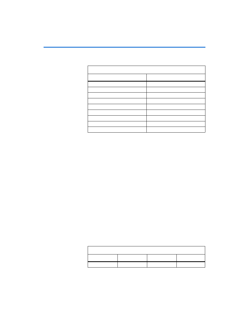
Table 2–3. Cyclone III Device Pin Count
Board Component
Pins
SRAM/flash (shared bus)
72
SDRAM (DDR)
Push-buttons
4
LEDs
USB-Blaster/configuration
4
HSMC
84
Total Pins Used
210
Total EP3C25F324 pins
214
Unused pins
4
Notes to
Table 2–3
:
(1)
The Cyclone III EP3C25F324 only supports one I/O standard in an I/O bank. I/O
banks 3 and 4 are shared among the DDR, HSMC and LEDs.
(2)
In several DDR designs, some of the I/O pins that share the same banks with the
DDR are unavailable for use due to different I/O standards. Therefore, if you
have added DDR to your system, I/O banks 3 and 4 is to be configured as SSTL-2
only while the HSMC and LEDs pins which are not using SSTL-2, should be
removed.
Table 2–4. Clock Pinout
Signal Name
FPGA Pin
Direction
Type
50 MHz
B9, V9
Input
2.5 V