Test designs, Configuring the fpga using quartus ii programmer – Altera Transceiver Signal Integrity User Manual
Page 17

December 2014
Altera Corporation
Transceiver Signal Integrity Development Kit,
Stratix IV GT Edition User Guide
6. Stratix IV GT Transceiver Signal
Integrity Demonstration
The kit installs a demonstration application and test designs. The application
provides an easy-to-use interface where you can select various transceiver settings
and observe the result. Before you run the application and test designs, connect the
USB cable to the board and navigate to the Stratix IV GT Transceiver Signal Integrity
Demonstration application as explained in
“Installing the Transceiver Signal Integrity
Development Kit, Stratix IV GT Edition” on page 3–1
Test Designs
Altera provides a set of SRAM Object File (.sof) test designs for the evaluation of the
Stratix IV GT device transceiver performance and board features. Before you run the
application, use the Quartus II Programmer to configure the Stratix IV GT device with
one of the .sof files.
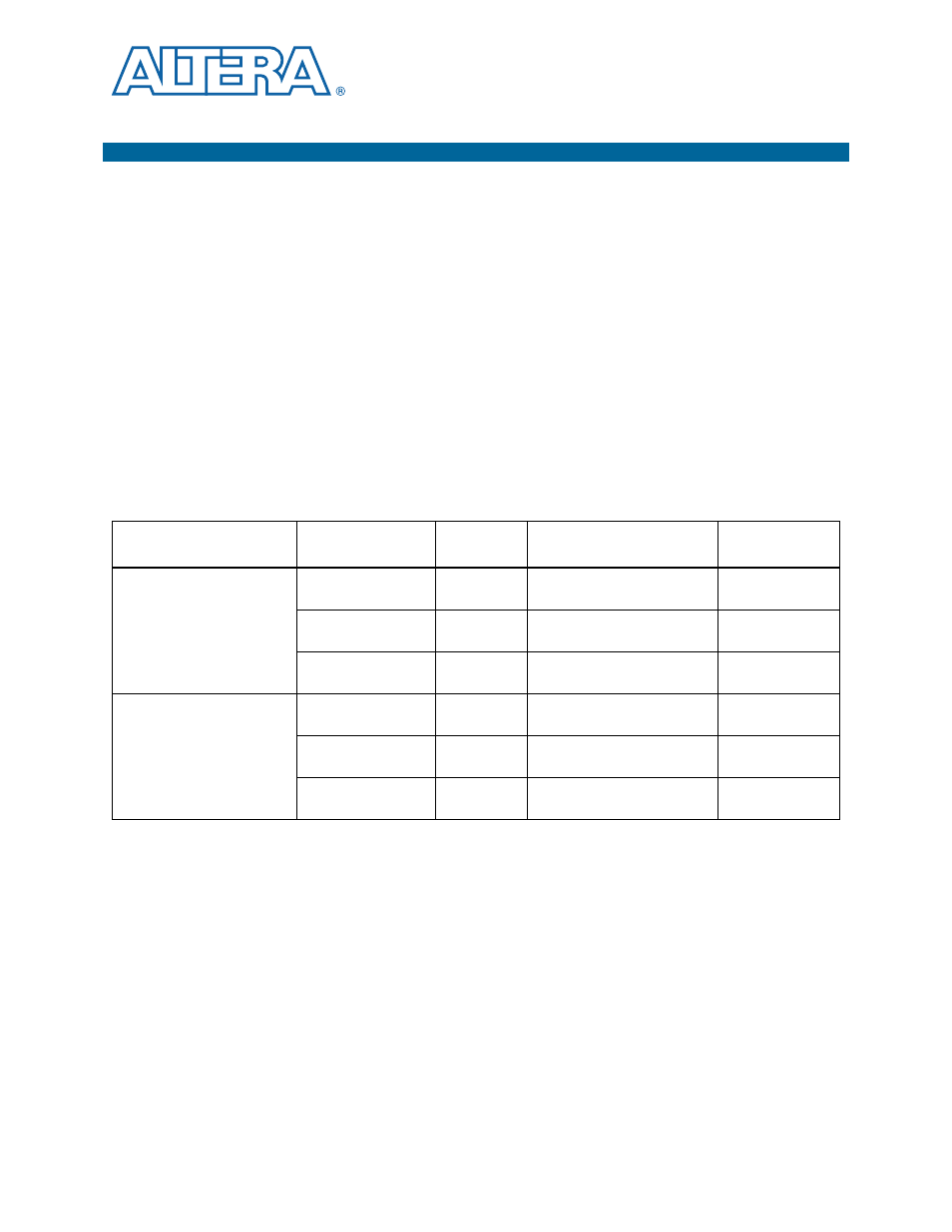
shows file name, data rate, transceiver mode, and clock
source details for each test design.
1
Early-release kits might not ship with the latest designs and new designs might be
added after kit release. Refer to
“Connecting to the Board Update Portal Web Page”
on page 5–1
to access the most current designs and revisions.
Configuring the FPGA Using Quartus II Programmer
It is sometimes necessary to use the Quartus II Programmer to configure the FPGA
with specific .sof files, such as the designs in
. Before configuring the FPGA,
ensure that the Quartus II Programmer and the USB-Blaster driver are installed on the
host computer and the development board is powered up.
Table 6–1. Test Design Details
File Name
Transceiver Block
and Channel
Data Rate
(Gbps)
Transceiver Mode
Clock Source
signal_integrity_demo1.sof
Block 2 Channel 0
11.3
Basic mode with low latency
PCS enabled (1)
Y4 (706.25 MHz)
Block 2 Channel 1
11.3
Basic mode with low latency
PCS enabled (1)
Y4 (706.25 MHz)
Block 1 Channels 2-5
10.3125
Basic mode with low latency
PCS enabled (1)
Y3 (644.53 MHz)
signal_integrity_demo2.sof
Block 2 Channel 0
11.3
Basic mode with low latency
PCS enabled (1)
Y4 (706.25 MHz)
Block 2 Channel 1
11.3
Basic mode with low latency
PCS enabled (1)
Y4 (706.25 MHz)
Block 1 Channels 6-9
10.3125
Basic mode with low latency
PCS enabled (1)
Y3 (644.53 MHz)
Note to
(1) This is the only transceiver mode available for the corresponding data rate.
