Custom instruction overview, Implementing custom instruction hardware, Custom instruction overview –2 – Altera Nios II Custom User Manual
Page 6: Implementing custom instruction hardware –2
1–2
Chapter 1: Nios II Custom Instruction Overview
Custom Instruction Overview
Nios II Custom Instruction User Guide
January 2011
Altera Corporation
Custom Instruction Overview
Nios II custom instructions are custom logic blocks adjacent to the ALU in the
processor’s datapath. Custom instructions give you the ability to tailor the Nios II
processor core to meet the needs of a particular application. You can accelerate time
critical software algorithms by converting them to custom hardware logic blocks.
Because it is easy to alter the design of the FPGA-based Nios II processor, custom
instructions provide an easy way to experiment with hardware-software tradeoffs at
any point in the design process.
Implementing Custom Instruction Hardware
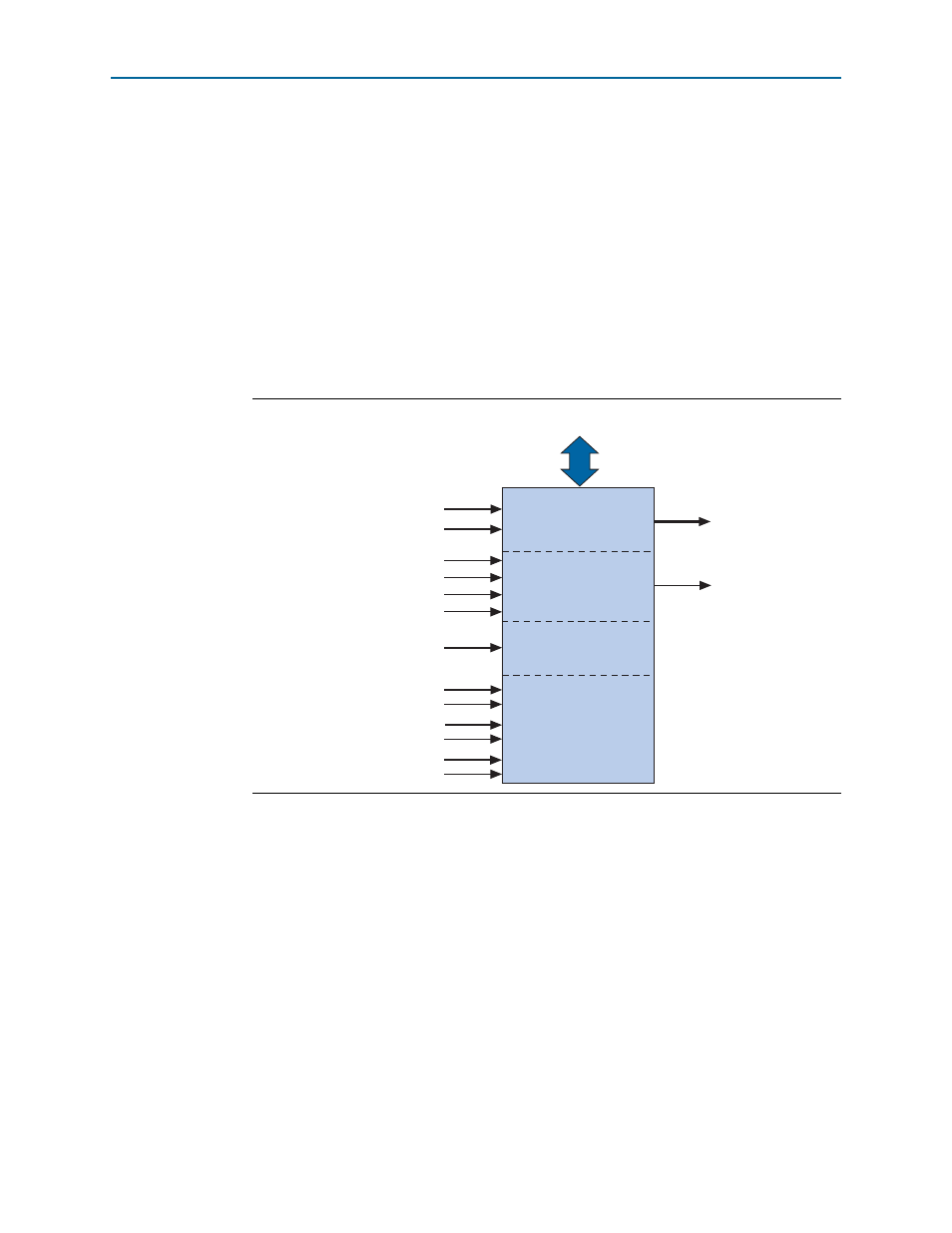
is a hardware block diagram of a Nios II custom instruction.
A Nios II custom instruction logic receives input on its
dataa
port, or on its
dataa
and
datab
ports, and drives out the result on its
result
port. The custom instruction logic
provides a result based on the inputs provided by the Nios II processor.
The Nios II processor supports different types of custom instructions.
lists
the additional ports that accommodate different custom instruction types. Only the
ports used for the specific custom instruction implementation are required.
also shows a conduit interface to external logic. The interface to external
logic allows you to include a custom interface to system resources outside of the
Nios II processor datapath.
Figure 1–2. Hardware Block Diagram of a Nios II Custom Instruction
Combinatorial
Conduit interface to external
memory, FIFO, or other logic
Multi-cycle
result
Extended
Internal
Register File
[31..0]
done
dataa[31..0]
datab[31..0]
clk
clk_en
reset
start
n[7..0]
a[4..0]
readra
b[4..0]
readrb
c[4..0]
writerc
Combinational
Custom
Logic