Factory default switch settings, Factory default switch settings –2 – Altera Cyclone V GX FPGA User Manual
Page 12
4–2
Chapter 4: Development Board Setup
Factory Default Switch Settings
Cyclone V GX FPGA Development Kit
October 2012
Altera Corporation
User Guide
f
For more information about the PFL megafunction, refer to
.
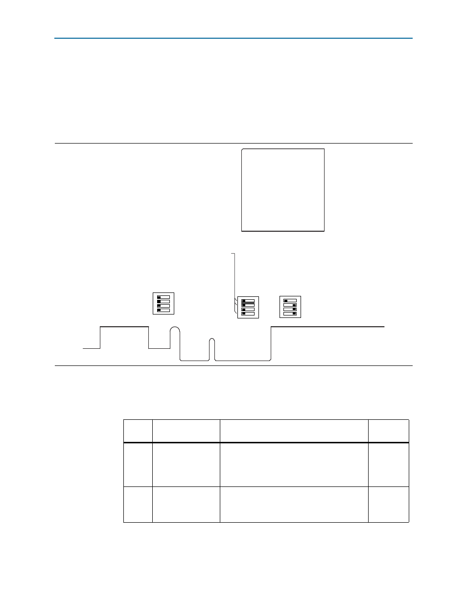
Factory Default Switch Settings
This section shows the factory switch settings (
) for the Cyclone V GX
FPGA development board.
To restore the switches to their factory default settings, perform these steps:
1. Set the DIP switch bank (SW3) to match
and
.
Figure 4–1. Switch Locations and Default Settings
SW3
CLK SEL
CLK EN
FACT LOAD
SEC MODE
PCIE_PRSNT2n_x1
PCIE_PRSNT2n_x4
-
FAN_FORCE_ON
SW5
5M2210_JTAG_EN
HSMA_JTAG_EN
PCIE_JTAG_EN
-
SW4
On
Off
On
Off
On
Off
ON
ON
ON
Table 4–1. SW3 DIP Switch Settings (Part 1 of 2)
Switch
Board
Label
Function
Default
Position
1
CLK SEL
Switch 1 has the following options:
■
On (0) = SMA input clock is selected.
■
Off (1) = Programmable oscillator clock is
selected.
Off
2
CLK EN
Switch 2 has the following options:
■
On (0) = On-board oscillator is disabled.
■
Off (1) = On-board oscillator is enabled.
Off
- MAX 10 JTAG (15 pages)
- MAX 10 Power (21 pages)
- Unique Chip ID (12 pages)
- Remote Update IP Core (43 pages)
- Device-Specific Power Delivery Network (28 pages)
- Device-Specific Power Delivery Network (32 pages)
- Hybrid Memory Cube Controller (69 pages)
- ALTDQ_DQS IP (117 pages)
- MAX 10 Embedded Memory (71 pages)
- MAX 10 Embedded Multipliers (37 pages)
- MAX 10 Clocking and PLL (86 pages)
- MAX 10 FPGA (26 pages)
- MAX 10 FPGA (56 pages)
- USB-Blaster II (22 pages)
- GPIO (22 pages)
- LVDS SERDES (27 pages)
- User Flash Memory (33 pages)
- ALTDQ_DQS2 (100 pages)
- Avalon Tri-State Conduit Components (18 pages)
- Cyclone V Avalon-MM (166 pages)
- Cyclone III FPGA Starter Kit (36 pages)
- Cyclone V Avalon-ST (248 pages)
- Stratix V Avalon-ST (286 pages)
- Stratix V Avalon-ST (293 pages)
- DDR3 SDRAM High-Performance Controller and ALTMEMPHY IP (10 pages)
- Arria 10 Avalon-ST (275 pages)
- Avalon Verification IP Suite (224 pages)
- Avalon Verification IP Suite (178 pages)
- FFT MegaCore Function (50 pages)
- DDR2 SDRAM High-Performance Controllers and ALTMEMPHY IP (140 pages)
- Floating-Point (157 pages)
- Integer Arithmetic IP (157 pages)
- Embedded Peripherals IP (336 pages)
- JESD204B IP (158 pages)
- Low Latency Ethernet 10G MAC (109 pages)
- LVDS SERDES Transmitter / Receiver (72 pages)
- Nios II Embedded Evaluation Kit Cyclone III Edition (3 pages)
- Nios II Embedded Evaluation Kit Cyclone III Edition (80 pages)
- IP Compiler for PCI Express (372 pages)
- Parallel Flash Loader IP (57 pages)
- Nios II C2H Compiler (138 pages)
- RAM-Based Shift Register (26 pages)
- RAM Initializer (36 pages)
- Phase-Locked Loop Reconfiguration IP Core (51 pages)
- DCFIFO (28 pages)