Design pcb decoupling using the pdn tool 2.0, Pre-layout instructions – Altera Device-Specific Power Delivery Network User Manual
Page 23

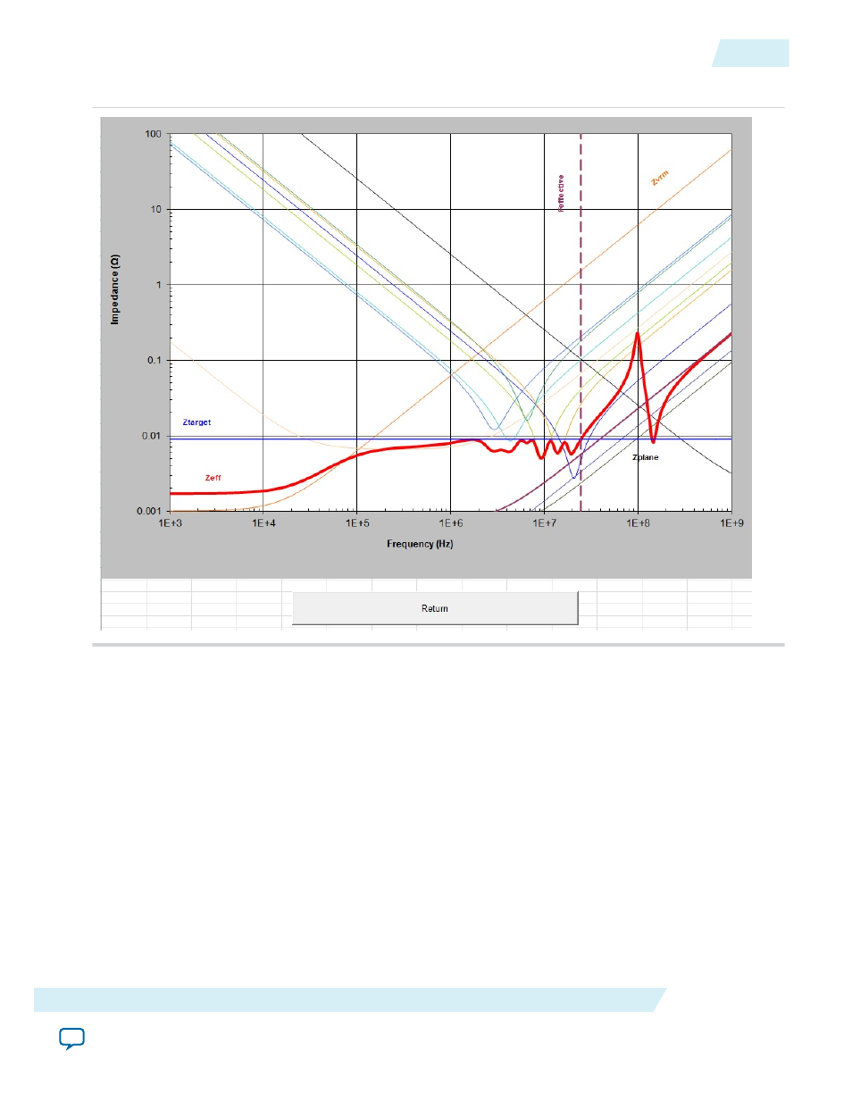
Figure 13: Enlarged_Graph Tab
Design PCB Decoupling Using the PDN Tool 2.0
PCB decoupling keeps PDN Z
EFF
smaller than Z
TARGET
with the properly chosen PCB capacitor combina‐
tion up to the frequency where the capacitor on the package and die take over the PDN decoupling. This
procedure uses the PDN tool 2.0 in different power rail configurations and provides design examples
using the Arria 10 device PDN tool.
Pre-Layout Instructions
The PDN tool 2.0 provides an accurate estimate of the number and types of capacitors needed to design a
robust power delivery network, regardless of where you are in the design phase. However, the accuracy of
the results depends highly on the user inputs for the various parameters.
If you have finalized the board stackup and have access to board database and layout information, you can
proceed through the tabs and enter the required information to arrive at an accurate decoupling scheme.
UG-01157
2015.03.06
Design PCB Decoupling Using the PDN Tool 2.0
23
Device-Specific Power Delivery Network (PDN) Tool 2.0 User Guide
Altera Corporation
