Stackup – Altera Device-Specific Power Delivery Network User Manual
Page 13
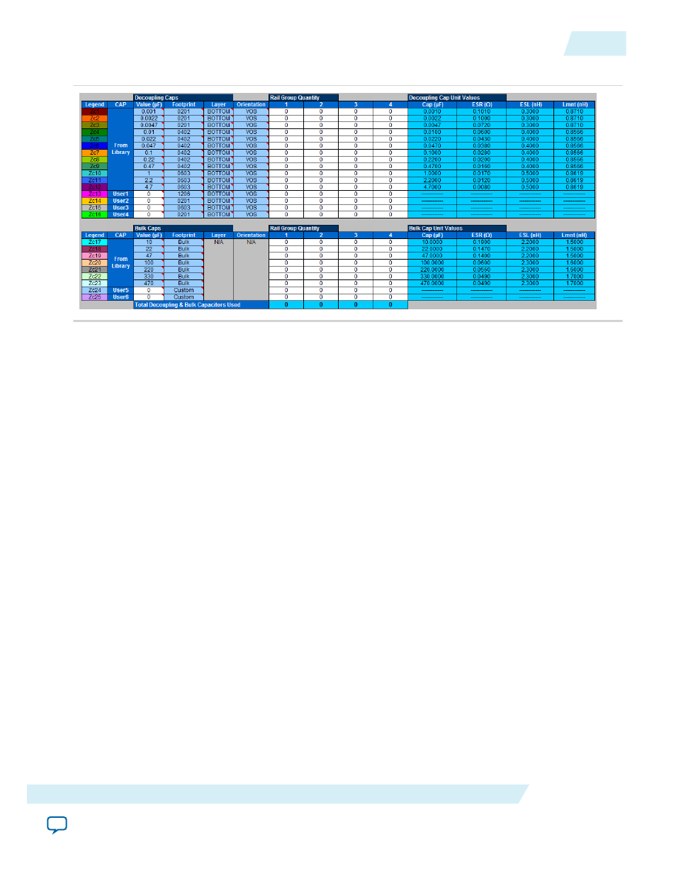
Figure 6: Results Summary Section of the System_Decap Tab
Recommended Flow for Deriving Decoupling for FPGA System using the System_Decap Tab
To use the System_Decap tab, perform the following steps:
1. Select the Altera device family or device.
2. Set up the stack up information in the Stackup tab.
3. Select the decoupling scheme.
The tool updates the power rail connection configuration to the scheme recommended in the Pin
Connection Guidelines.
4. Ensure that the following default parameters match your system, and make the necessary changes such
as:
• power rail configuration
• relativity of power rails within the same power group
• power group layer
• number of power/ground Via pairs
• DC voltage supply for VRM module
• decoupling cap location
5. Enter the projected current consumption of each power rail.
If you applied the Custom setting, refer to
on page 12 to enter your values.
Stackup
Enter the PCB stackup information of your design in the Stackup tab. This tab updates related data in the
BGA_Via, Plane_Cap, Cap_Mount and the X2Y_Mount tabs. The stackup information in this tab is also
used for the System_Decap tab. Follow the instructions provided at the beginning of the tab to fill in the
content for this tab.
UG-01157
2015.03.06
Recommended Flow for Deriving Decoupling for FPGA System using the
System_Decap Tab
13
Device-Specific Power Delivery Network (PDN) Tool 2.0 User Guide
Altera Corporation