Counter 0 counter 1 counter 2, 8254 timer/counter, 5 timer/counter operation – ADLINK PCM-9112+ User Manual
Page 49
Operation Theory
• 41
4.5 Timer/Counter
Operation
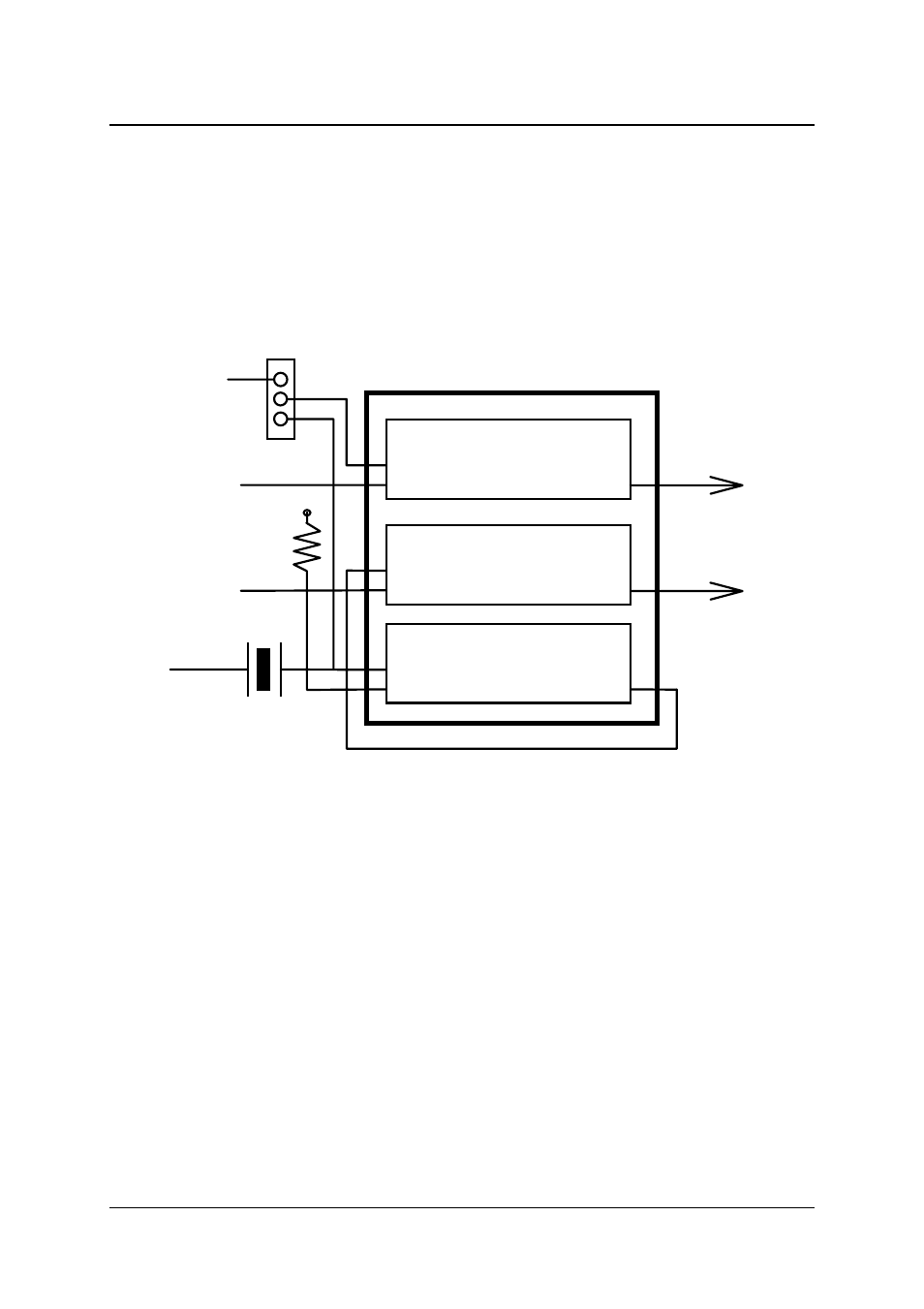
The PCI-9112 has an interval 8254 timer/counter on-board. It offers 3
independent 16-bit programmable down counters; counter 1 and counter 2
are cascaded together for A/D timer pacer trigger of A/D conversions, and
counter 0 is free for user applications. Figure 4.5 illustrates the 8254
timer/counter connections.
Counter 0
Counter 1
Counter 2
CLK0
GATE0
OUT0
CLK1
GATE1
CLK2
GATE2
OUT1
OUT2
2MHz
Oscillator
Vcc
A/D Trigger
CN3 Pin-34
CN3 Pin-37
CN3 Pin-33
CN3 Pin-16
CN3 Pin-35
INT
EXT
8254 Timer/Counter
Figure 4.5 Block Diagram of 8254 Timer/Counter
The clock source of counter 0 can be internal or external, while the gate can
be controlled externally and the output is send to connector CN3. As for
counter 1 and counter 2, the clock source is fixed internally; while the gate
can be controlled externally and the output is also send to connector CN3.
All timer/ counter signals are TTL compatible.
The following shows how to configure the 8254 timer / counter chip.
The 8254 Timer / Counter Chip
The Intel (NEC) 8254 contains three independent, programmable, multi-
mode 16 bit counter/timers. The three independent 16 bit counters can be
clocked at rates from DC to 5 MHz. Each counter can be individually
programmed with 6 different operating modes by appropriately formatted
control words. The most commonly uses for the 8254 in microprocessor-
based systems are: