ADLINK PCM-9112+ User Manual
Page 37
Registers
• 29
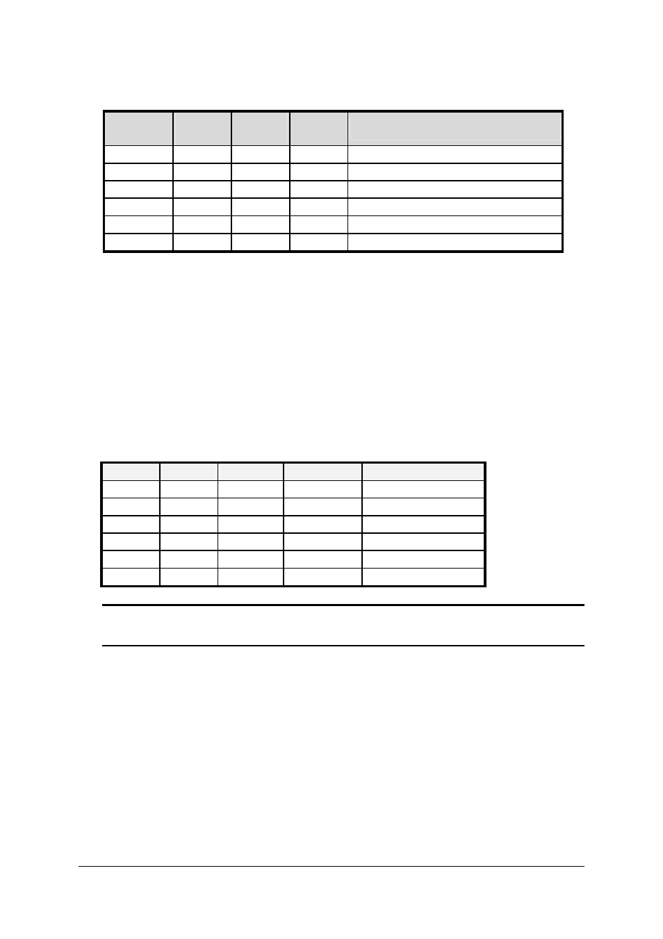
The modes below applies only to the PCI-9112 card:
Bit 3
EITS
Bit 2
TPST
Bit 1
INTX
Bit 0
DMAX
Mode & Description
0
0
0
0
Software Trigger & Polling
0
1
0
1
Timer Pacer Trigger & DMA
0
1
1
0
Timer Pacer Trigger & INT
1
X
0
0
External Trigger & Polling
1
X
0
1
External Trigger & DMA
1
X
1
0
External Trigger & INT
Auto-Scan: (Bit 4)
0: Auto Scan is disabled. Only channel [M3 M2 M1 M0] is converted only
1: The converted channel will be selected by the sequence [M3 M2 M1
M0] to 0, for example, the MUX register is [0110] and the auto-scan bit
is enabled, then the channel scan sequence is:
CH6, CH5, CH4, CH3, CH2, CH1, CH0, CH6, CH5,
MUX Register: (Bit8 ~ Bit5)
The converted A/D channel is controlled by the registers MUX, the format of
MUX is shown below.
Bit 8 M3 Bit 7 M2 Bit 6 M1
Bit 5 M0
Channel No.
0 0 0 0
CH0
0 0 0 1
CH1
0 0 1 0
CH2
... ... ... ...
...
1 1 1 0
CH14
1 1 1 1
CH15
Note: Single-ended mode: channel is selected from CH0 ~ CH15.
Differential mode: channel is selected from CH0 ~ CH7.