Vout vref dan = − × 4096, 3 d/a conversion – ADLINK PCM-9112+ User Manual
Page 47
Operation Theory
• 39
4.3 D/A
Conversion
The operation of the D/A conversion is less complex than the A/D operation.
You only need to write digital values into the D/A data registers and the
corresponding voltage will be outputted to AO1 or AO2. Refer to section 3.3
for information about the D/A data registers. The mathematical relationship
between the Digital number DAn and the output voltage is formulated as
follows:
Vout
Vref
DAn
= −
×
4096
Where the Vref is the reference voltage, the Vout is the output voltage, and
the DAn is the Digital value in the D/A data registers.
Before performing the D/A conversion, users should take care with the D/A
reference voltage, which is set by JP3 and JP4. Please refer to section 2.8
for jumper settings. The reference voltage will affect the output voltage. If the
reference voltage is -5V, the D/A output scaling will be 0~5V. If the reference
voltage is -10V, the D/A output scaling will be 0~10V.
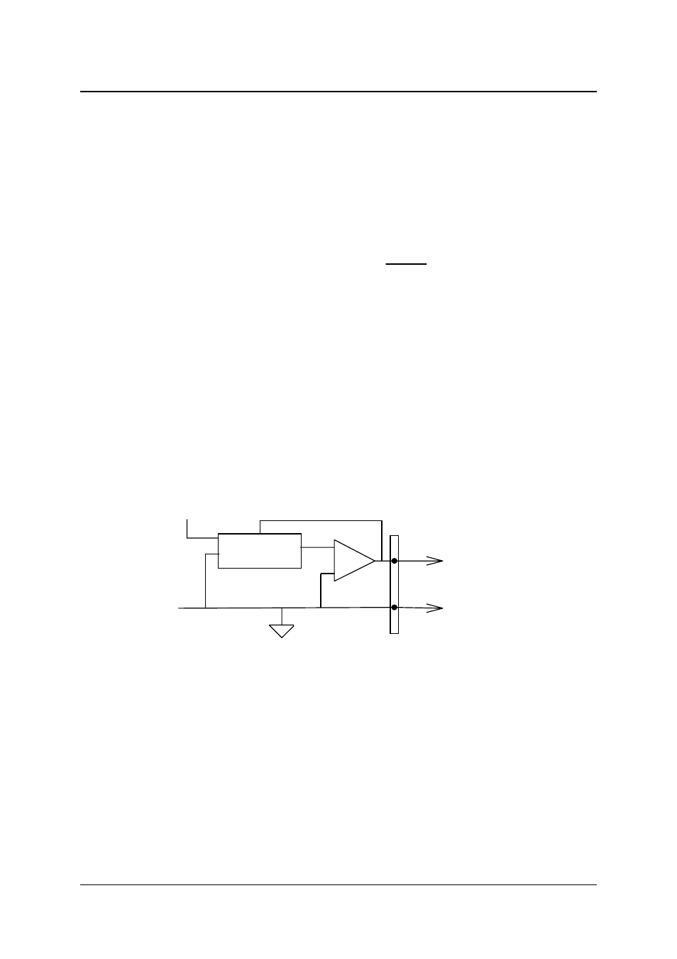
The PCI-9112 has two unipolar analog output channels. To make a D/A
output connection to the appropriate D/A output, please refer to Figure 4.3.
To D/A Output
D/A Converter
-
+
Ref In
-5 or -10
INT or Ext
Analog GND
Pin-30 ( AO0)
Pin-32 ( AO1)
Pin-14 ( A.GND)
Figure 4.3 Connection of Analog Output Connection
D/A Output