5 a/d status register – ADLINK PCM-9112+ User Manual
Page 38
30
• Registers
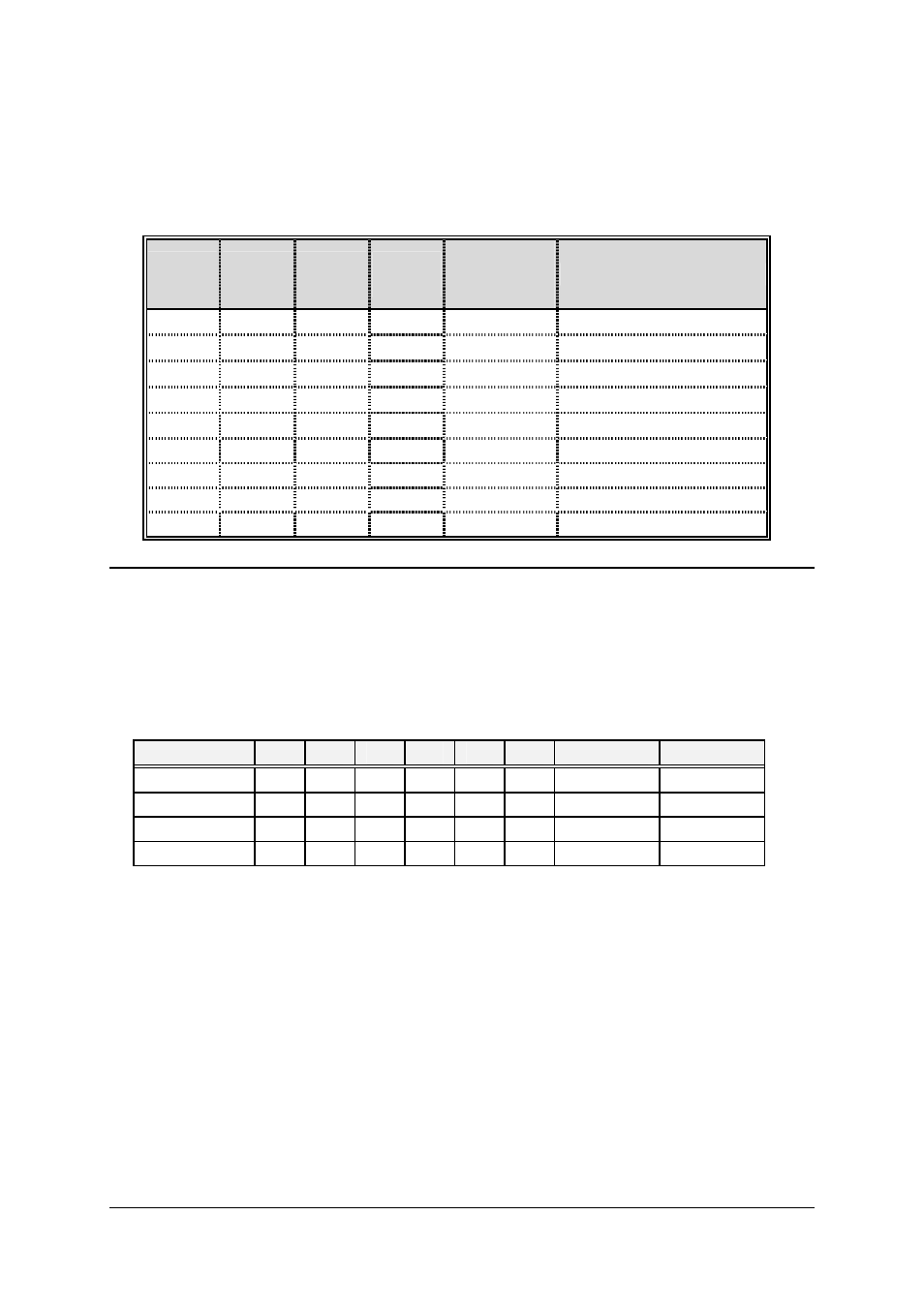
Gain: (Bit12 ~ Bit9)
With the PCI-9112, the analog input ranges are software programmable and
is controlled by the gain value. The gain values and its corresponding input
range are shown below.
(Bit12)
G3
(Bit11)
G2
(Bit10)
G1
(Bit9)
G0
Bipolar
or
Unipolar
Input Range
1 0 0 0 Bipolar
±10V
0 0 0 0 Bipolar
±5V
0 0 0 1 Bipolar
±2.5V
0 0 1 0 Bipolar
±1.25V
0 0 1 1 Bipolar
±0.625V
0 1 0 0
Unipolar 0V
~
10V
0 1 0 1
Unipolar
0V
~
5V
0 1 1 0
Unipolar 0V
~
2.5V
0 1 1 1
Unipolar 0V
~
1.25V
3.5 A/D
Status
Register
Address: BASE + 18
Attribute: read only
Data Format:
Bit
7
6
5
4
3
2
1
0
Base
+
18 --- --- --- --- --- --- DOVR DRDY
Base
+
19 --- --- --- --- --- ---
---
---
Base
+
1A --- --- --- --- --- ---
---
---
Base
+
1B --- --- --- --- --- ---
---
---
DOVR: A/D Over-Run (it can occur only when A/D is transferred in DMA bus
mastering mode).
1: A/D converted Data is over run
0: A/D converted Data is in normal condition
DRDY: A/D Data is Ready
1: A/D conversion is completed
0: A/D conversion is not completed