Cypress CY7C1332AV25 User Manual
Page 9
PRELIMINARY
CY7C1330AV25
CY7C1332AV25
Document No: 001-07844 Rev. *A
Page 9 of 19
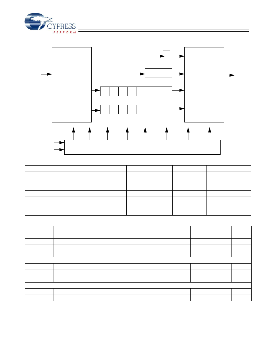
TAP Controller Block Diagram
TAP Electrical Characteristics
Over the Operating Range
[7, 8, 9]
Parameter
Description
Test Conditions
Min.
Max.
Unit
V
OH1
Output HIGH Voltage
I
OH
=
−2.0 mA
1.7
V
V
OH2
Output HIGH Voltage
I
OH
=
−100 µA
2.1
V
V
OL1
Output LOW Voltage
I
OL
= 2.0 mA
0.7
V
V
OL2
Output LOW Voltage
I
OL
= 100
µA
0.2
V
V
IH
Input HIGH Voltage
1.7
V
DD
+ 0.3
V
V
IL
Input LOW Voltage
–0.3
0.7
V
I
X
Input and Output Load Current
GND
≤ V
I
≤ V
DD
–5
5
µA
TAP AC Switching Characteristics
Over the Operating Range
[10, 11]
Parameter
Description
Min.
Max.
Unit
t
TCYC
TCK Clock Cycle Time
50
ns
t
TF
TCK Clock Frequency
20
MHz
t
TH
TCK Clock HIGH
20
ns
t
TL
TCK Clock LOW
20
ns
Set-up Times
t
TMSS
TMS Set-up to TCK Clock Rise
5
ns
t
TDIS
TDI Set-up to TCK Clock Rise
5
ns
t
CS
Capture Set-up to TCK Rise
5
ns
Hold Times
t
TMSH
TMS Hold after TCK Clock Rise
5
ns
t
TDIH
TDI Hold after Clock Rise
5
ns
Notes:
7. Minimum voltage equals –2.0V for pulse durations of less than 20 ns.
8. Input waveform should have a slew rate of > 1 V/ns.
9. These characteristics pertain to the TAP inputs (TMS, TCK, TDI and TDO). Parallel load levels are specified in the Electrical Characteristics Table.
10. t
CS
and t
CH
refer to the set-up and hold time requirements of latching data from the boundary scan register.
11. Test conditions are specified using the load in TAP AC test conditions. t
R
/t
F
= 1 ns.
0
0
1
2
.
.
29
30
31
Boundary Scan Register
Identification Register
0
1
2
.
.
.
.
106
0
1
2
Instruction Register
Bypass Register
Selection
Circuitry
Selection
Circuitry
TAP Controller
TDI
TDO
TCK
TMS