Pin definitions – Cypress CY7C1332AV25 User Manual
Page 3
PRELIMINARY
CY7C1330AV25
CY7C1332AV25
Document No: 001-07844 Rev. *A
Page 3 of 19
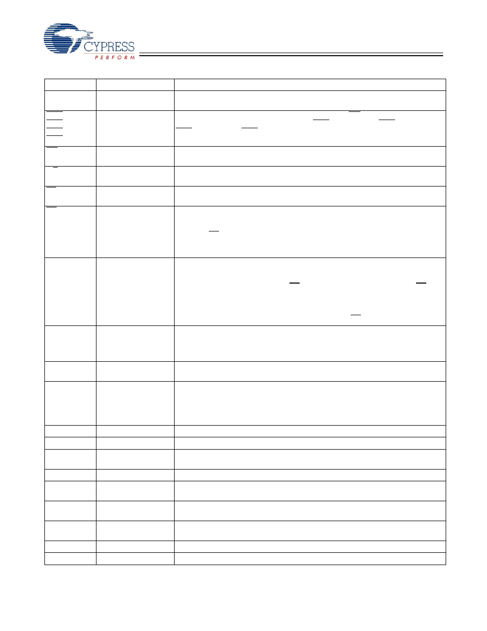
Pin Definitions
Name
I/O Type
Description
A
Input-
Synchronous
Address Inputs used to select one of the address locations. Sampled at the rising
edge of the K.
BWS
a
BWS
b
BWS
c
BWS
d
Input-
Synchronous
Byte Write Select Inputs, active LOW. Qualified with WE to conduct writes to the
SRAM. Sampled on the rising edge of CLK. BWS
a
controls DQ
a
, BWS
b
controls DQ
b
,
BWS
c
controls DQ
c
, BWS
d
controls DQ
d
.
WE
Input-
Synchronous
Write Enable Input, active LOW. Sampled on the rising edge of CLK. This signal must
be asserted LOW to initiate a write sequence and high to initiate a read sequence.
K,K
Input-
Differential Clock
Clock Inputs. Used to capture all synchronous inputs to the device.
CE
Input-
Synchronous
Chip Enable Input, active LOW. Sampled on the rising edge of CLK. Used to
select/deselect the device.
OE
Input-
Asynchronous
Output Enable, active LOW. Combined with the synchronous logic block inside the
device to control the direction of the I/O pins. When LOW, the I/O pins are allowed to
behave as outputs. When deasserted HIGH, I/O pins are tri-stated, and act as input
data pins. OE is masked during the data portion of a write sequence, during the first
clock when emerging from a deselected state and when the device has been
deselected.
DQ
a
DQ
b
DQ
c
DQ
d
I/O-
Synchronous
Bidirectional Data I/O lines. As inputs, they feed into an on-chip data register that is
triggered by the rising edge of CLK. As outputs, they deliver the data contained in the
memory location specified by A
[x:0]
during the previous clock rise of the read cycle. The
direction of the pins is controlled by OE and the internal control logic. When OE is
asserted LOW, the pins can behave as outputs. When HIGH, DQ
a
–DQ
d
are placed in
a tri-state condition. The outputs are automatically tri-stated during the data portion of
a write sequence, during the first clock when emerging from a deselected state, and
when the device is deselected, regardless of the state of OE. DQ a,b,c,d are 9 bits wide
M
1,
M
2
Read Protocol Mode
Pins
Mode control pins, used to set the proper read protocol. For specified device
operation, M
1
must be connected to V
SS
, and M
2
must be connected to V
DD
or V
DDQ
.
These mode pins must be set at power-up and cannot be changed during device
operation.
ZZ
Input-
Asynchronous
ZZ “sleep” Input. This active HIGH input places the device in a non-time critical “sleep”
condition with data integrity preserved.
ZQ
Input
Output Impedance Matching Input. This input is used to tune the device outputs to
the system data bus impedance. Q
[x:0]
output impedance are set to 0.2 x RQ, where
RQ is a resistor connected between ZQ and ground. Alternately, this pin can be
connected directly to V
DDQ
, which enables the minimum impedance mode. This pin
cannot be connected directly to GND or left unconnected.
V
DD
Power Supply
Power supply inputs to the core of the device. For this device, the V
DD
is 2.5V.
V
DDQ
I/O Power Supply
Power supply for the I/O circuitry. For this device, the V
DDQ
is 1.5V.
V
REF
Input-
Reference Voltage
Reference Voltage Input. Static input used to set the reference level for HSTL inputs
and Outputs as well as AC measurement points.
V
SS
Ground
Ground for the device. Should be connected to ground of the system.
TDO
JTAG serial output
Synchronous
Serial data-out to the JTAG circuit. Delivers data on the negative edge of TCK.
TDI
JTAG serial input
Synchronous
Serial data-in to the JTAG circuit. Sampled on the rising edge of TCK.
TMS
Test Mode Select
Synchronous
This pin controls the Test Access Port state machine. Sampled on the rising edge
of TCK.
TCK
JTAG serial clock
Serial clock to the JTAG circuit.
NC
–
No connects.