Cypress CY7C1332AV25 User Manual
Page 5

PRELIMINARY
CY7C1330AV25
CY7C1332AV25
Document No: 001-07844 Rev. *A
Page 5 of 19
guaranteed. The device must be deselected prior to entering
the “sleep” mode. CE must remain inactive for the duration of
t
ZZREC
after the ZZ input returns LOW.
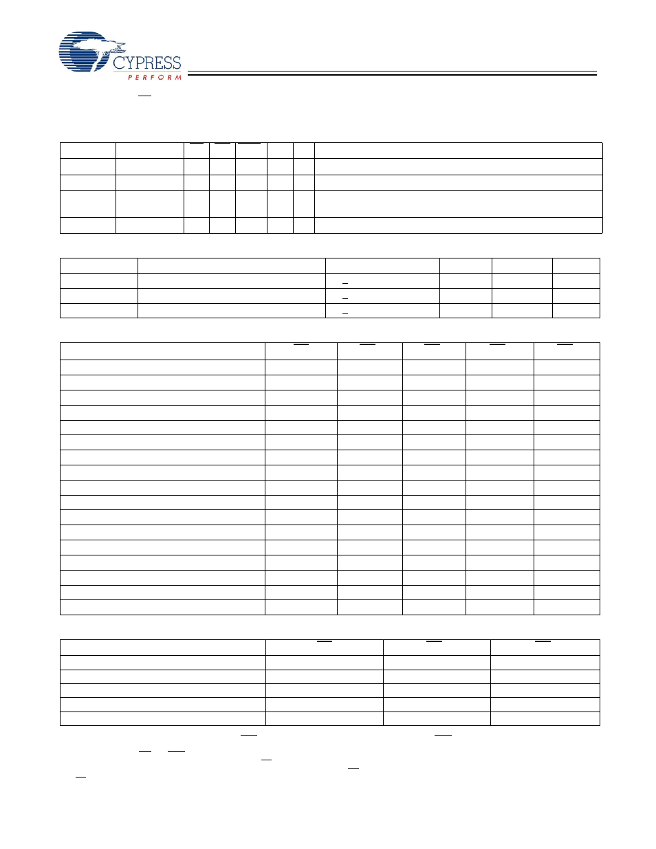
Cycle Description Truth Table
[1, 2, 3, 4, 5]
Operation Address Used CE
WE BWS
x
CLK ZZ
Comments
Deselected External
1
X
X
L-H
0
I/Os tri-state following next recognized clock.
Begin Read External
0
1
X
L-H
0
Address latched. Data driven out on the next rising edge of the clock.
Begin Write External
0
0
Valid
L-H
0
Address latched, data presented to the SRAM on the next rising
edge of the clock.
Sleep Mode
-
X
X
X
X
1
Power down mode.
ZZ Mode Electrical Characteristics
Parameter
Description
Test Conditions
Min.
Max.
Unit
I
DDZZ
Snooze mode standby current
ZZ > V
IH
128
mA
t
ZZS
Device operation to ZZ
ZZ > V
IH
2t
CYC
ns
t
ZZREC
ZZ recovery time
ZZ < V
IL
2t
CYC
ns
Write Cycle Descriptions
[1, 2]
Function (CY7C1330AV25)
WE
BW
d
BW
c
BW
b
BW
a
Read
1
X
X
X
X
Write Byte 0 – DQ
a
0
1
1
1
0
Write Byte 1 – DQ
b
0
1
1
0
1
Write Bytes 1, 0
0
1
1
0
0
Write Byte 2 – DQ
c
0
1
0
1
1
Write Bytes 2, 0
0
1
0
1
0
Write Bytes 2, 1
0
1
0
0
1
Write Bytes 2, 1, 0
0
1
0
0
0
Write Byte 3 – DQ
d
0
0
1
1
1
Write Bytes 3, 0
0
0
1
1
0
Write Bytes 3, 1
0
0
1
0
1
Write Bytes 3, 1, 0
0
0
1
0
0
Write Bytes 3, 2
0
0
0
1
1
Write Bytes 3, 2, 0
0
0
0
1
0
Write Bytes 3, 2, 1
0
0
0
0
1
Write All Bytes
0
0
0
0
0
Abort Write All Bytes
0
1
1
1
1
Write Cycle Descriptions
[1, 2]
Function (CY7C1332AV25)
WE
BW
b
BW
a
Read
1
X
X
Write Byte 0 – DQ
a
0
1
0
Write Byte 1 – DQ
b
0
0
1
Write All Bytes
0
0
0
Abort Write All Bytes
0
1
1
Notes:
1. X = “Don't Care,” 1 = Logic HIGH, 0 = Logic LOW. BWS
x
= 0 signifies at least one Byte Write Select is active, BWS
x
= Valid signifies that the desired byte write
selects are asserted, see Write Cycle Description table for details.
2. Write is defined by WE and BWS
x
. See Write Cycle Description table for details.
3. The DQ pins are controlled by the current cycle and the OE signal.
4. Device will power-up deselected and the I/Os in a tri-state condition, regardless of OE.
5. OE assumed LOW.
