Switching characteristics – Cypress CY7C1332AV25 User Manual
Page 15
PRELIMINARY
CY7C1330AV25
CY7C1332AV25
Document No: 001-07844 Rev. *A
Page 15 of 19
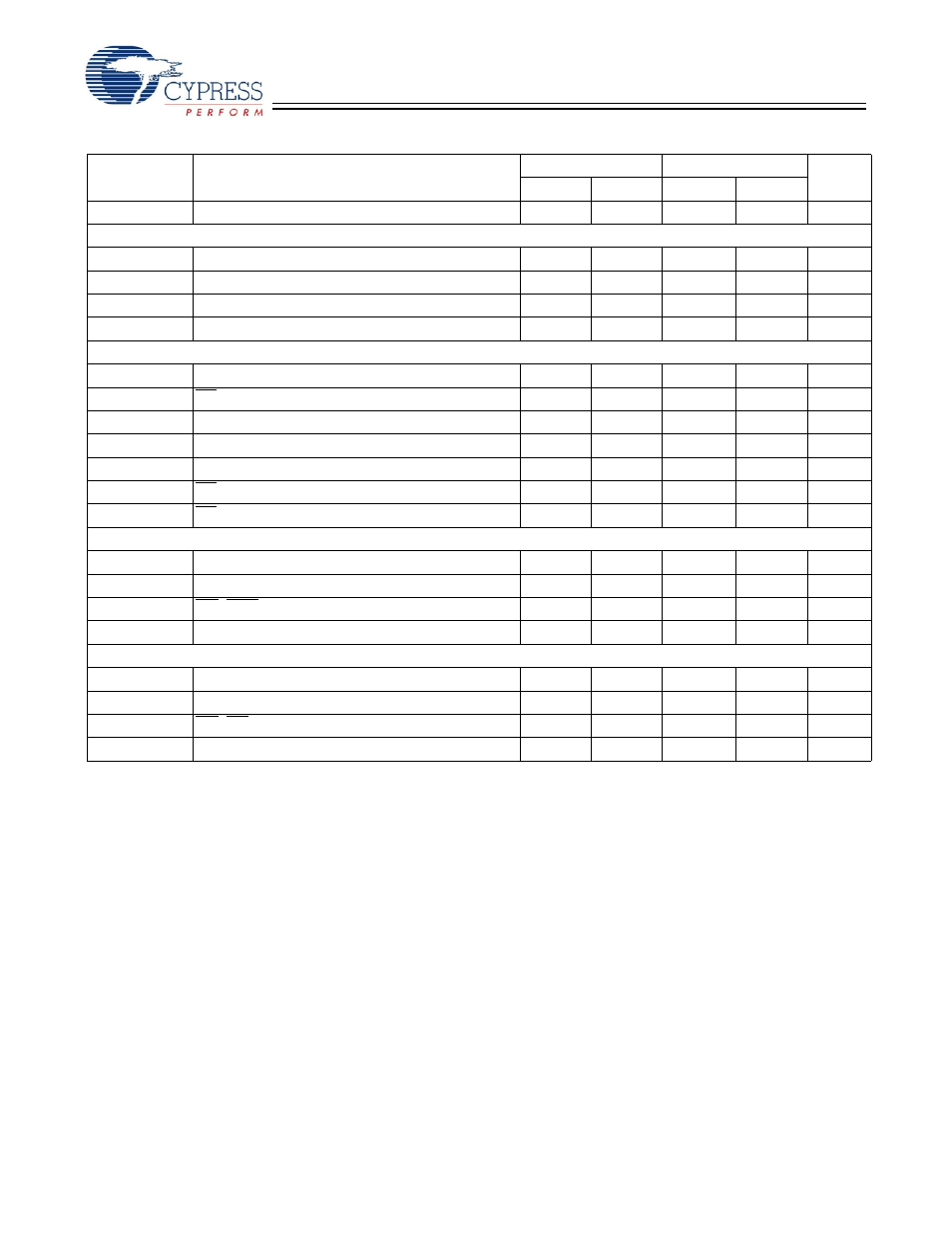
Switching Characteristics
[18, 19, 20, 21]
Parameter
Description
250
200
Unit
Min.
Max.
Min.
Max.
t
Power
V
CC
(typical) to the First Access Read or Write
[22]
1
1
ms
Clock
t
CYC
Clock Cycle Time
4.0
5.0
ns
F
MAX
Maximum Operating Frequency
250
200
MHz
t
CH
Clock HIGH
1.5
1.5
ns
t
CL
Clock LOW
1.5
1.5
ns
Output Times
t
CO
Data Output Valid After CLK Rise
2.0
2.25
ns
t
EOV
OE LOW to Output Valid
[17, 19, 21]
2.0
2.25
ns
t
DOH
Data Output Hold After CLK Rise
0.5
0.5
ns
t
CHZ
Clock to High-Z
[17, 18, 19, 20, 21]
2.0
2.25
ns
t
CLZ
Clock to Low-Z
[17, 18, 19, 20, 21]
0.5
0.5
ns
t
EOHZ
OE HIGH to Output High-Z
[18, 19, 21]
2.0
2.25
ns
t
EOLZ
OE LOW to Output Low-Z
[18, 19, 21]
0.5
0.5
ns
Set-Up Times
t
AS
Address Set-Up Before CLK Rise
0.3
0.3
ns
t
DS
Data Input Set-Up Before CLK Rise
0.3
0.3
ns
t
WES
WE, BWS
x
Set-Up Before CLK Rise
0.3
0.3
ns
t
CES
Chip Select Set-Up
0.3
0.3
ns
Hold Times
t
AH
Address Hold After CLK Rise
0.6
0.6
ns
t
DH
Data Input Hold After CLK Rise
0.6
0.6
ns
t
WEH
WE, BW
x
Hold After CLK Rise
0.6
0.6
ns
t
CEH
Chip Select Hold After CLK Rise
0.6
0.6
ns
Notes:
19. t
CHZ
, t
CLZ
, are specified with a load capacitance of 5 pF as in part (b) of AC Test Loads. Transition is measured
± 100 mV from steady-state voltage.
20. At any given voltage and temperature, t
EOHZ
is less than t
EOLZ
and t
CHZ
is less than t
CLZ
to eliminate bus contention between SRAMs when sharing the same
data bus. These specifications do not imply a bus contention condition, but reflect parameters guaranteed over worst case user conditions. Device is designed
to achieve High-Z prior to Low-Z under the same system conditions.
21. This parameter is sampled and not 100% tested.
22. This part has a voltage regulator that steps down the voltage internally; t
Power
is the time power needs to be supplied above V
DD
minimum initially before a read
or write operation can be initiated.