Pin configurations, Ball bga pinout, Pin definitions – Cypress CY7C1350G User Manual
Page 3

CY7C1350G
Document #: 38-05524 Rev. *F
Page 3 of 15
Pin Configurations
(continued)
2
3
4
5
6
7
1
A
B
C
D
E
F
G
H
J
K
L
M
N
P
R
T
U
DQ
A
V
DDQ
NC/576M
NC/1G
DQ
C
DQ
D
DQ
C
DQ
D
A
A
A
A
NC/18M
V
DDQ
CE
2
A
V
DDQ
V
DDQ
V
DDQ
V
DDQ
NC/144M
NC
A
DQ
C
DQ
C
DQ
D
DQ
D
NC
V
DD
A
NC/72M
DQP
D
A
A
ADV/LD
A
CE
3
NC
V
DD
A
A
NC
V
SS
V
SS
NC
DQP
B
DQ
B
DQ
B
DQ
A
DQ
B
DQ
B
DQ
A
DQ
A
NC
NC
NC
V
DDQ
NC
V
SS
V
SS
V
SS
V
SS
V
SS
V
SS
V
SS
V
SS
MODE
CE
1
V
SS
OE
V
SS
V
DDQ
BW
C
NC/9M
V
SS
WE
V
DDQ
V
DD
V
SS
V
DD
V
SS
CLK
NC
BW
A
CEN
V
SS
V
DDQ
V
SS
ZZ
NC/288M
A
A
A1
A0
V
SS
V
DD
DQP
C
DQ
B
A
NC/36M
DQ
C
DQ
B
DQ
C
DQ
C
DQ
C
DQ
B
DQ
B
DQ
A
DQ
A
DQ
A
DQ
A
DQP
A
DQ
D
DQ
D
DQ
D
DQ
D
BW
D
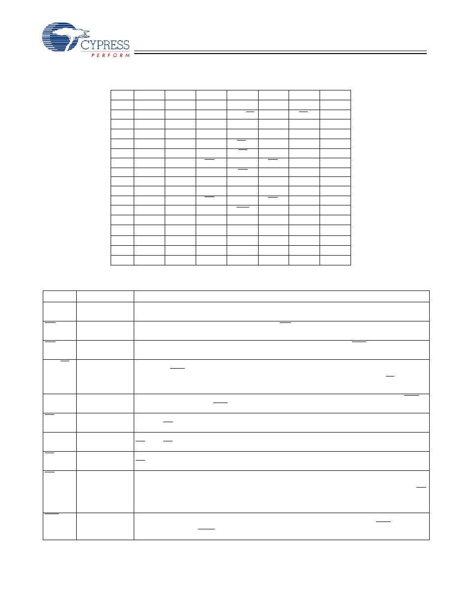
119-Ball BGA Pinout
BW
B
NC
Pin Definitions
Name
I/O
Description
A0, A1, A
Input-
Synchronous
Address Inputs used to select one of the 128K address locations. Sampled at the rising edge
of the CLK. A
[1:0]
are fed to the two-bit burst counter.
BW
[A:D]
Input-
Synchronous
Byte Write Inputs, active LOW. Qualified with WE to conduct writes to the SRAM. Sampled on
the rising edge of CLK.
WE
Input-
Synchronous
Write Enable Input, active LOW. Sampled on the rising edge of CLK if CEN is active LOW. This
signal must be asserted LOW to initiate a write sequence.
ADV/LD
Input-
Synchronous
Advance/Load Input. Used to advance the on-chip address counter or load a new address. When
HIGH (and CEN is asserted LOW) the internal burst counter is advanced. When LOW, a new
address can be loaded into the device for an access. After being deselected, ADV/LD should be
driven LOW in order to load a new address.
CLK
Input-Clock
Clock Input. Used to capture all synchronous inputs to the device. CLK is qualified with CEN.
CLK is only recognized if CEN is active LOW.
CE
1
Input-
Synchronous
Chip Enable 1 Input, active LOW. Sampled on the rising edge of CLK. Used in conjunction with
CE
2
and CE
3
to select/deselect the device.
CE
2
Input-
Synchronous
Chip Enable 2 Input, active HIGH. Sampled on the rising edge of CLK. Used in conjunction with
CE
1
and CE
3
to select/deselect the device.
CE
3
Input-
Synchronous
Chip Enable 3 Input, active LOW. Sampled on the rising edge of CLK. Used in conjunction with
CE
1
and
CE
2
to select/deselect the device.
OE
Input-
Asynchronous
Output Enable, asynchronous input, active LOW. Combined with the synchronous logic block
inside the device to control the direction of the I/O pins. When LOW, the I/O pins are allowed to
behave as outputs. When deasserted HIGH, I/O pins are tri-stated, and act as input data pins. OE
is masked during the data portion of a write sequence, during the first clock when emerging from
a deselected state, when the device has been deselected.
CEN
Input-
Synchronous
Clock Enable Input, active LOW. When asserted LOW the Clock signal is recognized by the
SRAM. When deasserted HIGH the Clock signal is masked. Since deasserting CEN does not
deselect the device, CEN can be used to extend the previous cycle when required.
