Truth table, Write cycle descriptions – Cypress CY7C1302DV25 User Manual
Page 5
CY7C1302DV25
Document #: 38-05625 Rev. *A
Page 5 of 18
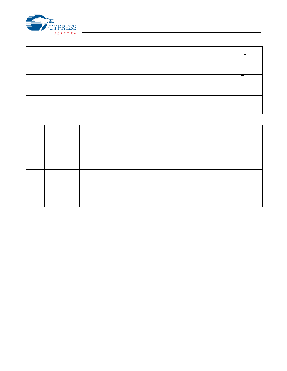
Truth Table
[2, 3, 4, 5, 6, 7]
Operation
K
RPS
WPS
DQ
DQ
Write Cycle:
Load address on the rising edge of K
clock; input write data on K and K rising
edges.
L-H
X
L
D(A+0) at K(t)
↑
D(A+1) at K(t)
↑
Read Cycle:
Load address on the rising edge of K
clock; wait one cycle; read data on 2
consecutive C and C rising edges.
L-H
L
X
Q(A+0) at C(t+1)
↑
Q(A+1) at C(t+1)
↑
NOP: No Operation
L-H
H
H
D = X
Q = High-Z
D = X
Q = High-Z
Standby: Clock Stopped
Stopped
X
X
Previous State
Previous State
Write Cycle Descriptions
[2,8]
BWS
0
BWS
1
K
K
Comments
L
L
L-H
–
During the Data portion of a Write sequence, both bytes (D
[17:0]
) are written into the device.
L
L
–
L-H
During the Data portion of a Write sequence, both bytes (D
[17:0]
) are written into the device.
L
H
L-H
–
During the Data portion of a Write sequence, only the lower byte (D
[8:0]
) is written into the
device. D
[17:9]
remains unaltered.
L
H
–
L-H
During the Data portion of a Write sequence, only the lower byte (D
[8:0]
) is written into the
device. D
[17:9]
remains unaltered.
H
L
L-H
–
During the Data portion of a Write sequence, only the byte (D
[17:9]
) is written into the device.
D
[8:0]
remains unaltered.
H
L
–
L-H
During the Data portion of a Write sequence, only the byte (D
[17:9]
) is written into the device.
D
[8:0]
remains unaltered.
H
H
L-H
–
No data is written into the device during this portion of a Write operation.
H
H
–
L-H
No data is written into the device during this portion of a Write operation.
Notes:
2. X = Don't Care, H = Logic HIGH, L = Logic LOW,
↑
represents rising edge.
3. Device will power-up deselected and the outputs in a three-state condition.
4. “A” represents address location latched by the devices when transaction was initiated. A+0, A+1 represent the addresses sequence in the burst.
5. “t” represents the cycle at which a Read/Write operation is started. t+1 is the first clock cycle succeeding the “t” clock cycle.
6. Data inputs are registered at K and K rising edges. Data outputs are delivered on C and C rising edges, except when in single clock mode.
7. It is recommended that K = K and C = C when clock is stopped. This is not essential, but permits most rapid restart by overcoming transmission line charging
symmetrically. 38-05625
8. Assumes a Write cycle was initiated per the Write Port Cycle Description Truth Table. BWS
0
, BWS
1
can be altered on different portions of a Write cycle, as long
as the set-up and hold requirements are achieved. 38-05625